
Method of controlling power conversion device

a power conversion device and control method technology, applied in the direction of dc-ac conversion without reversal, power conversion systems, electrical appliances, etc., can solve the problems of large switching loss, reduced efficiency of power conversion devices, and loss of switching, so as to reduce switching loss, suppress sudden change of noise, and reduce noise

Inactive Publication Date: 2012-02-09
MEIDENSHA ELECTRIC MFG CO LTD
View PDF7 Cites 7 Cited by
  • Summary
  • Abstract
  • Description
  • Claims
  • Application Information

AI Technical Summary

Benefits of technology

The present invention relates to a method for reducing loss in a power conversion device by controlling the switching of semiconductor switches in a power conversion device. The invention proposes a two-arm modulation method that reduces switching loss while maintaining good waveform control. The invention also addresses the problem of excessive heat generation in the device caused by the high switching frequency. The technical effects of the invention include improved efficiency, reduced size of the device, and improved performance.

Problems solved by technology

When an on-off operation of a semiconductor switching element, i.e., a switching of the semiconductor switching element is conducted in a power conversion device (for example, a three-phase inverter), a switching loss is caused.
In a case that this switching loss is large, is there is a problem such as an efficiency decrease of the power conversion device and an upsizing of the power conversion device because of the necessity of a cooling device for removing a generated heat.

Method used


Image

  • Method of controlling power conversion device
  • Method of controlling power conversion device
  • Method of controlling power conversion device

Examples


first embodiment

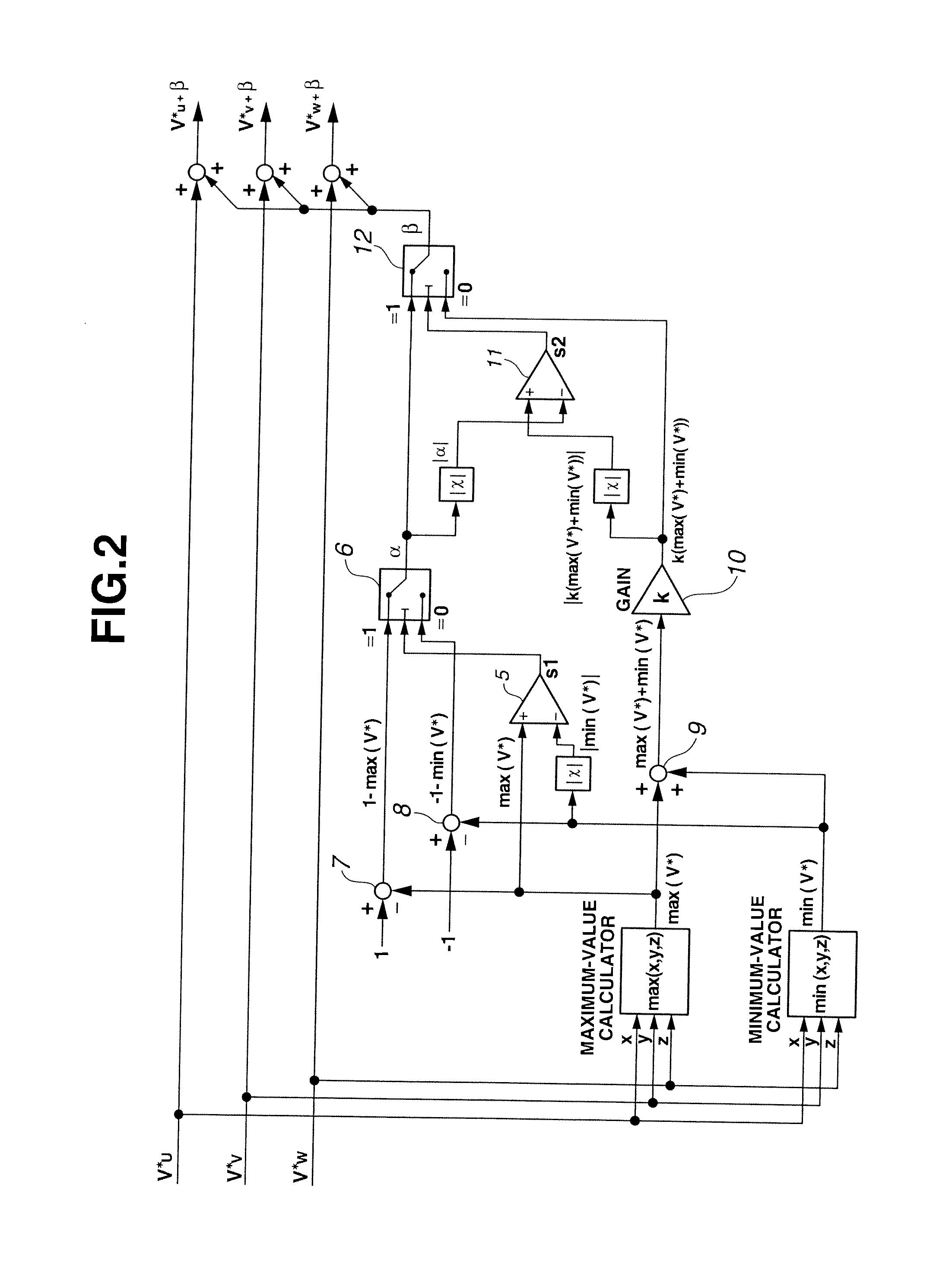
[0046]Voltage command values V*U, V*V and V*W of three phases are inputted to a gate-signal generating section shown in FIG. 1. This gate-signal generating section outputs gate signals to semiconductor switching elements provided in a power conversion device (for example, a three-phase inverter) for performing an AC-to-DC conversion or DC-to-AC conversion. Each of the gate signals is obtained by applying a pulse-width modulation (PWM) to the voltage command value. A correction-term adder 1 adds a second correction amount (hereinafter referred to as, correction amount β to each of the voltage command values V*U, V*V and V*W of three phases, and thereby produces corrected voltage command values V*U+β, V*V+β and V*W+β, as shown in FIG. 2. Then, the correction-term adder 1 outputs the corrected voltage command values V*Uβ, V*V+β and V*W+β respectively to comparators 2. Since operations of a NOT-circuit 3 and a dead-time generating circuit 4 provided downstream of the comparator 2 in FIG...

second embodiment

[0089]In the modulation method of the first embodiment, the correction amount β is added to the three-phase voltage command values V*U, V*V and V*W. Thereby, a zero-phase voltage (i.e., a voltage to ground) is varied. However, the variation of the voltage to ground is increased, a leakage current become problematic.

[0090]Therefore, in a second embodiment according to the present invention, the gain k of the modulation method of the first embodiment is varied according to the modulation factor m.

[0091]A concrete example of the case where gain k is varied according to the modulation factor m will now be explained. FIG. 8 (a) is a time chart of the U-phase voltage command value V*U in a case that the modulation factor m is increased from 0 to 1.15 with a constant gradient. FIG. 8 (b) is a time chart of the correction amount α and the signal k(max(V*)+min(V*)). FIG. 8 (c) is a time chart of the gain k. FIG. 8 (d) is a time chart of the correction amount β. FIG. 8 (e) is a time chart of ...

third embodiment

[0095]In the second embodiment, the mixture ratio between the three-arm modulation method and the two-arm modulation method is varied in accordance with a magnitude of the modulation factor m. However, in a third embodiment according to the present invention, the mixture ratio between the three-arm modulation method and the two-arm modulation method is varied in accordance with not only the modulation factor m but also a load factor l of the power conversion device.

[0096]A main loss of the power conversion device can be classified into a conduction loss and the switching loss. FIG. 9 is an explanatory view of the switching loss. A following formula (5) represents a loss wsw per one switching. A following formula (6) represents a switching loss Wsw per unit time. For simplicity's sake, the following explanations will be given assuming that a voltage v and a current i vary linearly as shown in FIG. 9.

[Formula 5]

wsw∫Tswv·idt[J]  (5)

[Formula 6]

Wsw=fsw·∫Tswv·idt[W]  (6)

[0097]In such a ca...


PUM


Abstract

A correction-term adder 1 compares a maximum value max(V*) with an absolute value of a minimum value min(V*). The correction-term adder 1 selects a signal 1−max(V*) when the maximum value max(V*) is larger than the absolute value of the minimum value min(V*), on the other hand, selects a signal −1−min(V*) when the absolute value of the minimum value min(V*) is larger than the maximum value max(V*). Thereby, a signal of correction amount α is calculated. Moreover, the correction-term adder 1 produces a triangular-wave-shaped signal k(max(V*)+min(V*)) by multiplying a gain k by an addition signal max(V*)+min(V*) of the maximum value max(V*) and the minimum value min(V*). This triangular-wave-shaped signal k(max(V*)+min(V*)) is synchronized with the correction amount α. The correction-term adder 1 produces a correction amount β by selecting smaller one in absolute value between the triangular-wave-shaped signal k(max(V*)+min(V*)) and the correction amount α, and adds the correction amount β to the voltage command values V*U, V*V, V*W.

Description

TECHNICAL FIELD[0001]The present invention relates to a pulse-width modulation (PWM) control reducing a loss in a power conversion device for converting alternating current into direct current or direct current into alternating current.BACKGROUND ART[0002]When an on-off operation of a semiconductor switching element, i.e., a switching of the semiconductor switching element is conducted in a power conversion device (for example, a three-phase inverter), a switching loss is caused. In a case that this switching loss is large, is there is a problem such as an efficiency decrease of the power conversion device and an upsizing of the power conversion device because of the necessity of a cooling device for removing a generated heat. Contrary to this, in a case that a switching frequency is lowered in order to reduce the switching loss, a waveform-control performance is reduced due to a decrease of the number of switching operations. That is, a rate of higher harmonics relative to a fundam...

Claims


Application Information

Patent Timeline
Patent Type & Authority Applications(United States)
IPC IPC(8): H02M7/00
CPCH02M7/219H02M2001/0025H02M7/53875H02M1/0025H02M7/48
Inventor MUNESHIMA, MASAKAZUYAMAMOTO, YASUHIROSASAKI, YUSUGAI, TAKUYASHIGAKI, AKIRA
Owner MEIDENSHA ELECTRIC MFG CO LTD
Learn More