Display apparatus

a display apparatus and diode technology, applied in the direction of instruments, static indicating devices, etc., can solve the problems of increasing power consumption of display apparatus, consuming capacitor electricity, leakage current, etc., and achieves the effect of reducing power consumption, maximizing driving methods, and reducing power consumption

Active Publication Date: 2012-01-26
INNOLUX CORP
View PDF6 Cites 10 Cited by
  • Summary
  • Abstract
  • Description
  • Claims
  • Application Information

AI Technical Summary

Benefits of technology

[0012]As mentioned above, in the display apparatus of the present invention, each pixel has a memory circuit for storing the image data during a frame time. Accordingly, the image data can be remained in the memory circuit of the pixel without continuously receiving the image data from the data line. Therefore, the memory of the source driver is unnecessary to continuously store the pixel data and output it to the corresponding pixel, so that it is not needed to apply additional power to the source driver in this circumstance. Thus, the power consumption can be reduced. To be noted, the benefit of this driving method is maximized especially at the partial dimmed lit mode.
[0013]Moreover, the display apparatus of the present invention further includes a mode switching circuit for switching the control mode between a normal mode and a Memory-In-Pixel (MIP) mode. Accordingly, the display apparatus of the present invention can be driven based on the above-mentioned driving method with lower power consumption or the conventional driving method, so that the applications of the invention can be further broadened.

Problems solved by technology

However, the leakage current issue may occur in both the n-type thin-film transistor 11 and the p-type thin-film transistor 12, which will consume the electricity stored in the capacitor 13.
Nevertheless, the power consumption of the display apparatus is increased.

Method used


Image

  • Display apparatus
  • Display apparatus
  • Display apparatus

Examples


Embodiment Construction

[0024]The present invention will be apparent from the following detailed description, which proceeds with reference to the accompanying drawings, wherein the same references relate to the same elements.

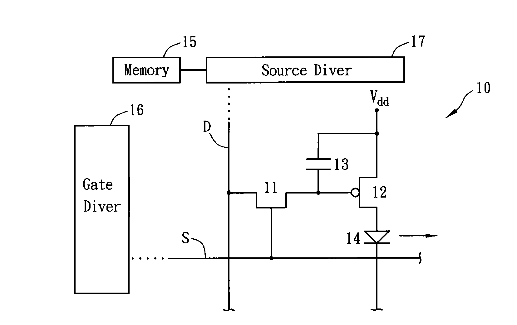
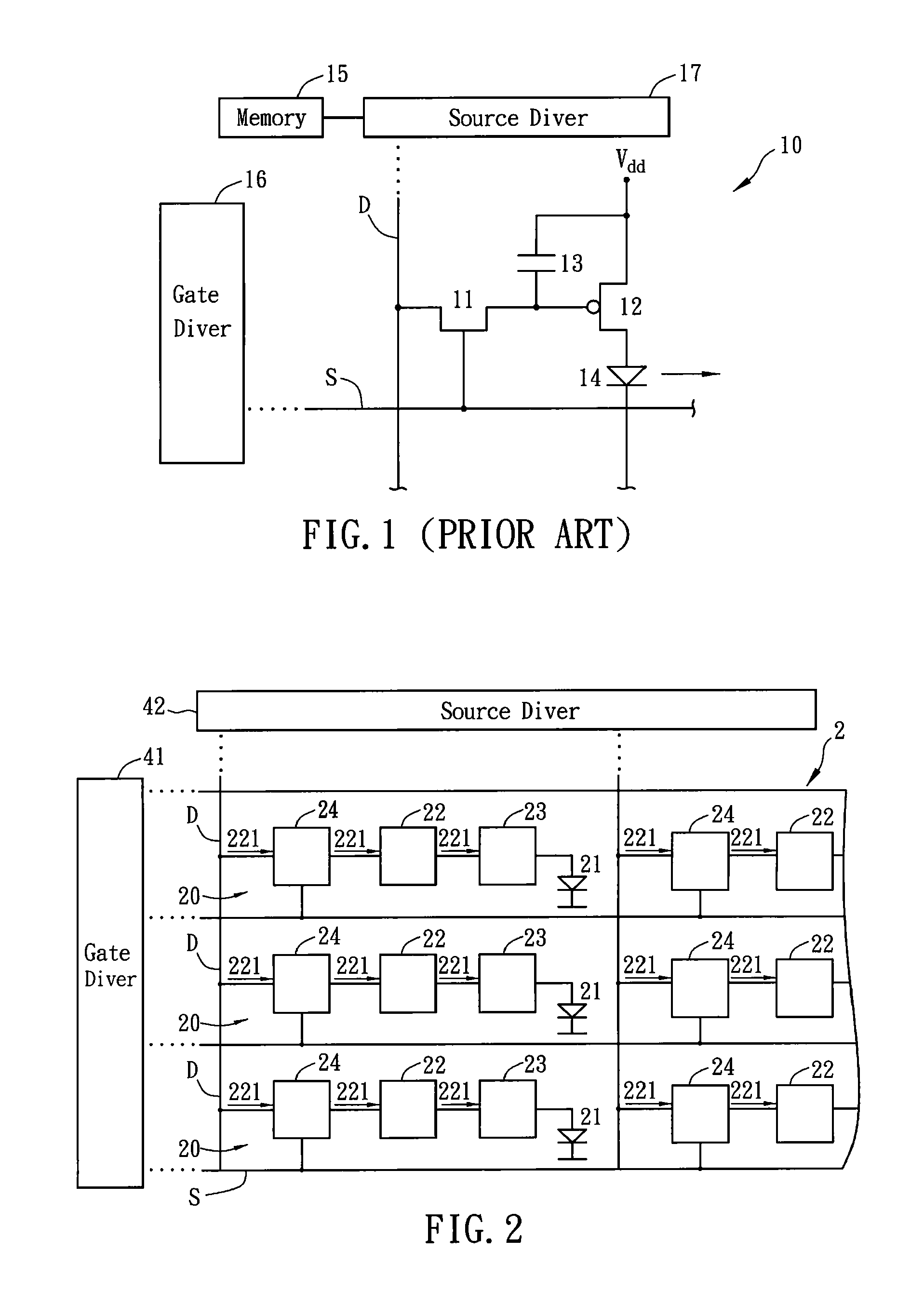
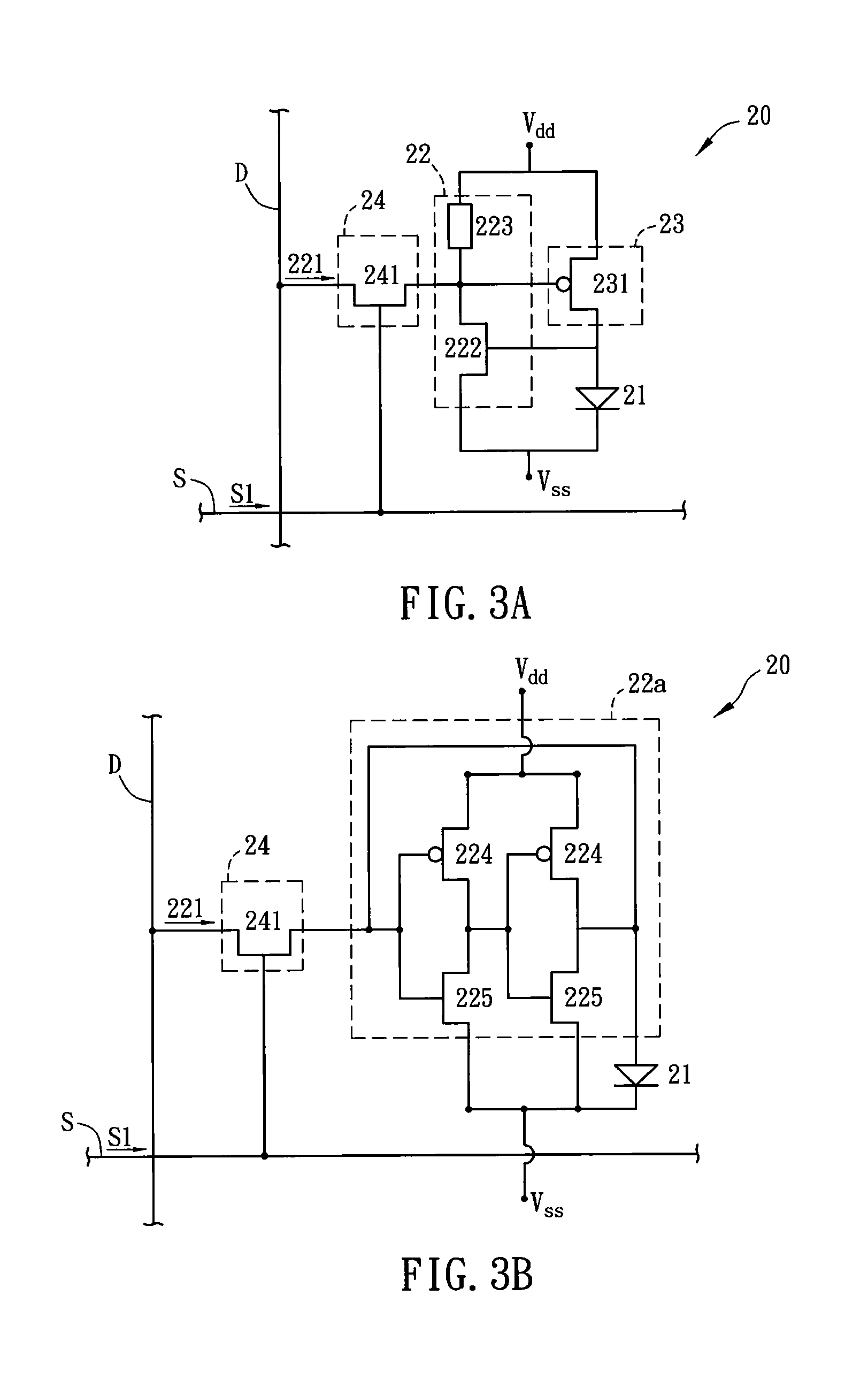
[0025]FIG. 2 is a block diagram showing the circuit of a display apparatus according to an embodiment of the present invention. With reference to FIG. 2, a display apparatus 2 includes a plurality of pixels 20, and each pixel 20 includes a light emitting unit 21, a memory circuit 22, and a driving circuit 23.

[0026]The memory circuit 22 can store an image data 221, and the driving circuit 23 is electrically connected with the light emitting unit 21 and the memory circuit 22 for driving the light emitting unit 21 according to the image data 221.

[0027]The pixels 20 are arranged in matrix, and every three pixels 20, for example, can construct a pixel unit. To be noted, the pixels 20 may also be arranged in a polygonal shape or other shape, and the pixel unit may be constructed by differen...


PUM


Abstract

A display apparatus includes a plurality of pixels. Each pixel has a light emitting unit, a memory cell, and a driving circuit. The memory cell stores an image data. The driving circuit is electrically connected with the light emitting unit and the memory cell, and drives the light emitting unit according to the image data.

Description

[0001]This application claims the benefit of U.S. Provisional Patent Application No. 61 / 233,862 entitled Circuit for memory and use of the same in active matrix devices, inventor Keitaro Yamashita, filed Aug. 14, 2009, and incorporated herein by reference.BACKGROUND OF THE INVENTION[0002]1. Field of Invention[0003]The invention relates to a display apparatus and, in particular, to an organic light-emitting diode (OLED) display apparatus.[0004]2. Related Art[0005]Recently, the OLED with various advantages, such as high brightness, full color, wide viewing angle, self-emission, fast response speed, flexibility, simple manufacturing process, low cost, etc., is developed. Compared with the liquid crystal display technology, the OLED display apparatus is a better choice with considering the property requirements of flat display apparatuses.[0006]FIG. 1 is a schematic diagram showing the pixel circuit 10 in a conventional OLED display apparatus. As shown in FIG. 1, the pixel circuit 10 co...

Claims


Application Information

Patent Timeline
Patent Type & Authority Applications(United States)
IPC IPC(8): G09G3/30G09G3/20
CPCG09G3/3225G09G2330/021G09G2300/0857G09G2300/0842
Inventor YAMASHITA, KEITARO
Owner INNOLUX CORP
Why Eureka
Try Eureka