Stacked multi-chip

Active Publication Date: 2012-01-12
NATIONAL TSING HUA UNIVERSITY
View PDF28 Cites 8 Cited by
  • Summary
  • Abstract
  • Description
  • Claims
  • Application Information

AI Technical Summary

Benefits of technology

[0005]The objective of the present invention is to provide a stacked multi-level chip that has good thermal dissipation, is easy to construct fully-stacked TSV for all chips and is easy to position voltage level shifters.

Problems solved by technology

However, the conventional stacked multi-chip that uses TSV technology has three problems: inadequate thermal dissipation, difficulty to constructing fully-stacked TSV for all chips and difficulty of placing voltage level shifters.

Method used


Image

  • Stacked multi-chip
  • Stacked multi-chip
  • Stacked multi-chip

Examples


Embodiment Construction

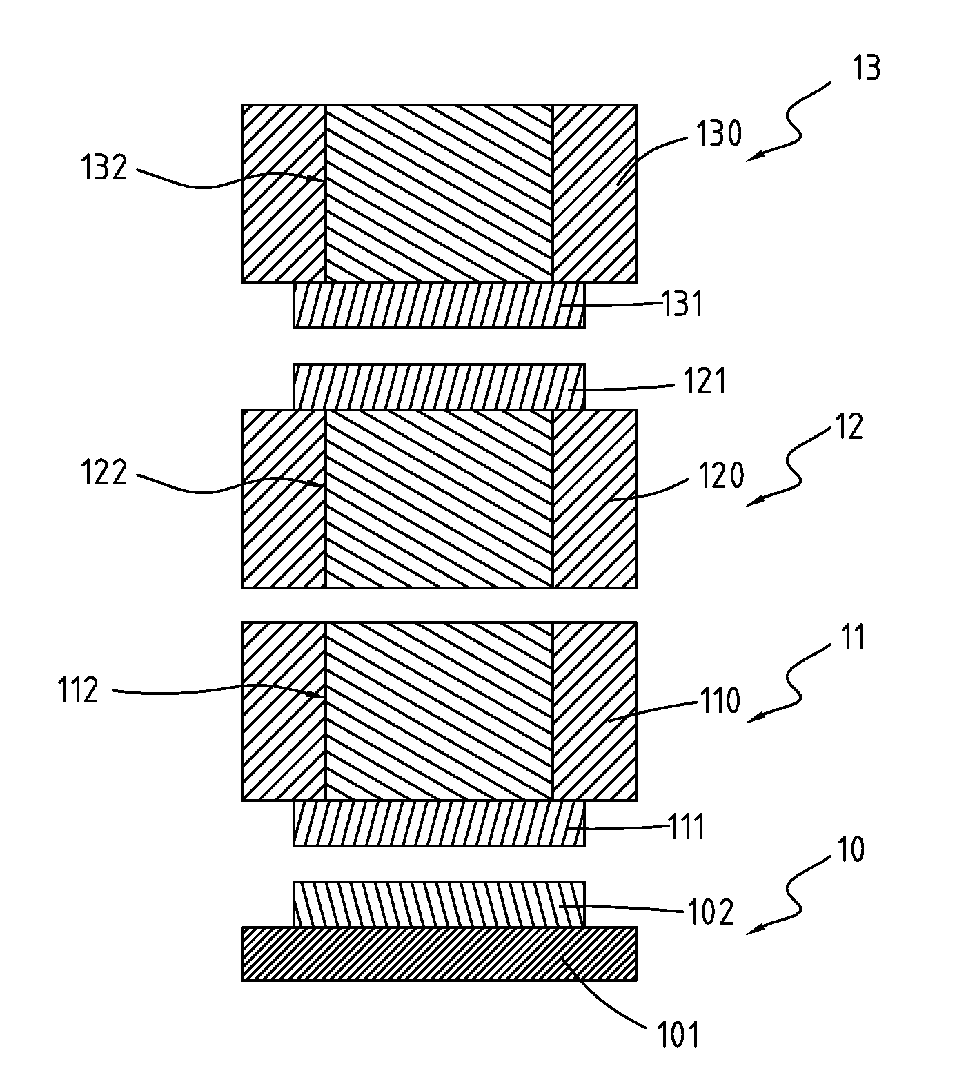
[0013]With reference to FIG. 1, a stacked multi-chip in accordance with the present invention has good thermal dissipation, is easy to construct fully-stacked TSV for all chips, allows voltage level shifters to be easily positioned and comprises a base layer (10), a first chip (11), a first stacked chip (12) and at least one second stacked chip (13).

[0014]The base layer (10) comprises a mounting panel (101) and a redistributed layer (102). The mounting panel (101) is non-conductive and has an outer surface and an inner surface. The outer surface is mounted in an electrical device. The redistributed layer (102) is mounted on the inner surface of the mounting panel (101), has a top surface and may use metal wire mounted on the top surface.

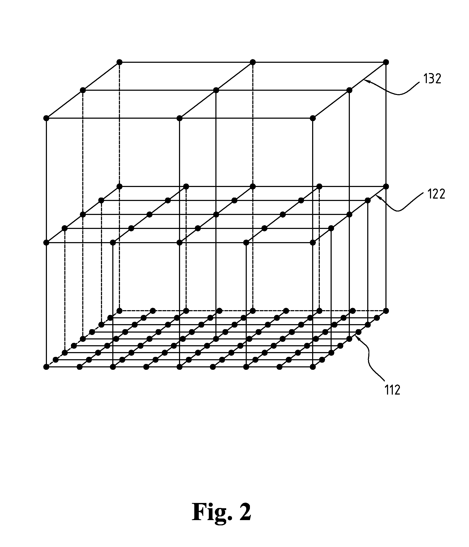
[0015]With further reference to FIGS. 2 and 3, the first chip (11) comprises an electrically non-conductive layer (110) and a connective layer (111). The electrically non-conductive layer (110) has a top surface and a bottom surface, may be silicon a...


PUM


Abstract

A stacked multi-chip comprises a base layer, a first chip, a first stacked chip and at least one second stacked chip. The base layer comprises a mounting panel and a redistributed layer. The redistributed layer is mounted on the mounting panel. The first chip comprises an electrically non-conductive layer and a connective layer. The electrically non-conductive layer comprises a TSV channel. The connective layer abuts the redistributed layer. The first stacked chip is mounted on the first chip and comprises an electrically non-conductive layer and a connective layer. The electrically non-conductive layer comprises a TSV channel that is connected to the TSV channel of the first chip. The second stacked chip is mounted on the first stacked chip and comprises an electrically non-conductive layer and a connective layer. The electrically non-conductive layer comprises a TSV channel. The connective layer is connected to the connective layer of the first stacked chip.

Description

FIELD OF THE INVENTION[0001]The present invention is a stacked multi-chip.BACKGROUND OF THE INVENTION[0002]In high-density electrical interconnections, a conventional stacked multi-chip achieves better performance in speed and power by using Through Silicon Via (TSV) technology to stack several chips and give the stacked multi-chip high performance, high density and smaller dimensions. For example, U.S. Pat. No. 7,091,592 B2 discloses a semiconductor chip that uses TSV in a stacked multi-chip.[0003]However, the conventional stacked multi-chip that uses TSV technology has three problems: inadequate thermal dissipation, difficulty to constructing fully-stacked TSV for all chips and difficulty of placing voltage level shifters.[0004]Accordingly, what is needed in the art is a new design of the stacked multi-chip that uses TSV technology to have good thermal dissipation, be easy to construct fully-stacked TSV for all chips and be easy to position voltage level shifters.SUMMARY OF THE IN...

Claims


Application Information

Patent Timeline
IPC IPC(8): H01L23/48
CPCH01L23/481H01L23/5286H01L25/0657H01L2223/6616H01L2223/6666H01L2924/0002H01L2225/06513H01L2225/06544H01L2924/00
Inventor HWANG, TING-TINGHSIEN-TE, CHEN
Owner NATIONAL TSING HUA UNIVERSITY
Why Eureka
Try Eureka