Systems and methods for material layer identification through image processing

a technology of image processing and material layer, applied in image enhancement, image data processing, instruments, etc., can solve the problems of inability to locate and identify single and few-layer graphene regions in graphene samples, inability to analyze large-area graphene wafers, and limited existing methods

Inactive Publication Date: 2011-12-08
RGT UNIV OF CALIFORNIA
View PDF2 Cites 28 Cited by
  • Summary
  • Abstract
  • Description
  • Claims
  • Application Information

AI Technical Summary

Benefits of technology

[0009]In an embodiment, a computer-implemented method for identifying a number of layers in a layered thin film material. The method comprises, under control of one or more computing devices receiving a first electronic image comprising a representation of at least a portion of a first layered thin film material in a selected color space captured under one or more selected illumination conditions. The method further comprises determining a correlation between a number of layers of the layered thin film material and a range of color component values of the selected color space. The method additionally comprises receiving a second electronic image comprising a representation of at least a portion of a second layered thin film material in the selected color space captured under the one or more selected illumination conditions, wherein the second layered thin film material comprises the same material as the first layered thin film material. The method further comprises identifying a number of layers in a selected region of the second electronic image of the second layered thin film material using the determined first correlation.
[0010]In another embodiment, a computer-implemented method for identifying a number of layers in a layered thin film material is provided. The method comprises receiving an electronic image comprising a representation of at least a portion of a first layered thin film material in a selected color space captu

Problems solved by technology

Unfortunately, locating and identifying regions of single and few-layer graphene regions in graphene samples is currently problematic.
For example, existing methods may be limited owing to their relatively slow, expensive, and non-automated measurement procedures.
These methods may also become impractical and / or inadequate for analyzing large-area graphene wafers (e.g., lateral length scales on the order of millimeters), which is practical for industrial processes.
Moreover, most of these techniques provide only rough estimates of the number of atomic layers.
This difficulty in identifying the number of atomic layers of graphene is of concern because the physical characteristics of FLG are different from those of SLG.
As a result, the one-atom thickness of graphene and its optical transparency (approximately.3% absorption per layer) make graphene identification and counting the number of atomic planes in FLG extremely challenging.
However, as graphene of larger areas becomes available, quality control remains as an important factor that may limit further progress in graphene research and applications of graphene and other layered materials.

Method used


Image

  • Systems and methods for material layer identification through image processing
  • Systems and methods for material layer identification through image processing
  • Systems and methods for material layer identification through image processing

Examples


Embodiment Construction

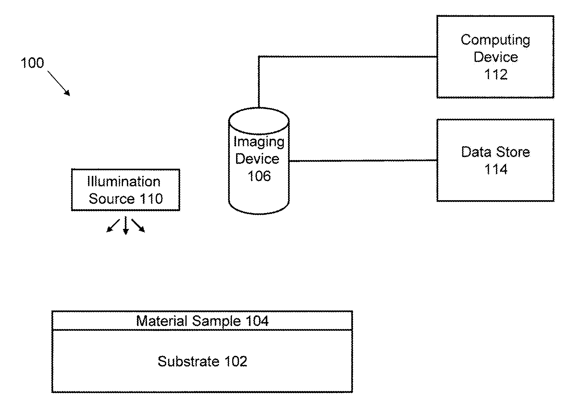
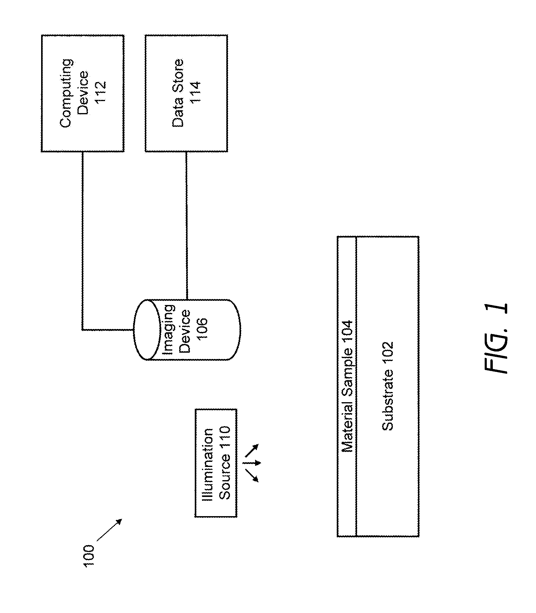
[0024]Embodiments of the present disclosure relate to systems and methods for the detection of a number of layers present in selected thin film materials. In certain embodiments, the materials may comprise layers that are coupled by Van der Waals forces. In further embodiments, the materials may comprise graphene, topological insulators (e.g., Bi2Te3, BiSe3), thermoelectrics (e.g., Bi2Te3), mica, materials having a Van der Waals gap and that may be exfoliated, and materials having a Van der Waals gap and that may be grown (e.g., grown by techniques including, but not limited to, chemical vapor deposition (CVD), molecular beam epitaxy (MBE), atomic layer deposition (ALP), and the like. Embodiments of the systems and methods may be discussed below in the context of graphene, however, the embodiments of the disclosure may be applied to any layered materials

[0025]The terms “approximately,”“about,” and “substantially” as used herein represent an amount close to the stated amount that sti...


PUM


Abstract

A fast and fully automated approach for determining the number of atomic planes in layered material samples is provided. Examples of such materials may include graphene and bismuth telluride (Bi2Te3), and materials from the bismuth selenide (Bi2Se3) samples is provided. The disclosed procedure allows for in situ identification of the borders of the regions with the same number of atomic planes. The procedure is based on an image processing algorithm that employs micro-Raman calibration, light background subtraction, correction for lighting non-uniformity, and color and grayscale image processing on each pixel of a graphene image. The developed procedure may further provide a pseudo-color map that marks the single-layer and few-layer regions of the sample. Beneficially, embodiments of the developed procedure may be employed using various substrates and can be applied to materials that are mechanically exfoliated, chemically derived, or deposited on an industrial scale.

Description

CROSS-REFERENCE TO RELATED APPLICATIONS[0001]This application claims the benefit of priority under 35 U.S.C. §119(e) of U.S. Provisional Application No. 61 / 315,343, filed on Mar. 18, 2010, and entitled “SYSTEMS AND METHODS FOR GRAPHENE IDENTIFICATION THROUGH IMAGE PROCESSING,” the entirety of which is hereby incorporated by reference and should be considered a part of this specification.BACKGROUND OF THE INVENTION[0002]1. Field of the Invention[0003]Embodiments of the present disclosure pertain to systems and methods for materials characterization and, in particular, to identification of layers in atomically thin materials, such as graphene and graphene-like exfoliated thin film materials.[0004]2. Description of the Related Art[0005]Graphene is a two-dimensional (2-D) crystal of sp2-bonded carbon atoms. Mechanical exfoliation of graphene has lead to the identification that graphene possesses high electronic, thermal, optical and mechanical properties. These outstanding properties ma...

Claims


Application Information

Patent Timeline
IPC IPC(8): G06K9/00
CPCG01N21/25G01N21/65G01N21/8422G06T7/0081G06T2207/30148G06T2207/10056G06T2207/10116G06T2207/20032G06T2207/30108G06T7/0097G06T7/11G06T7/174
Inventor NOLEN, CRAIG MERTENDENINA, GIOVANNI LAVISTETEWELDEBRHAN, DESALEGNE B.BALANDIN, ALEXANDER A.BHANU, BIR
Owner RGT UNIV OF CALIFORNIA
Why Eureka
Try Eureka