Substrate for light emitting element package, and light emitting element package

a technology of light emitting elements and substrates, which is applied in the direction of basic electric elements, electrical equipment, semiconductor devices, etc., can solve the problems of high processing cost, and achieve the effects of high heat conductivity, efficient conductivity, and efficient conductivity

Inactive Publication Date: 2011-11-10
DENKA CO LTD
View PDF4 Cites 5 Cited by
  • Summary
  • Abstract
  • Description
  • Claims
  • Application Information

AI Technical Summary

Benefits of technology

[0021]On the other hand, a light emitting element package of the present invention comprises: the above substrate for a light emitting element package; a light emitting element mounted above said thick metal section; and a sealing resin for sealing the light emitting element. Therefore, the heat generated in the light emitting element is efficiently conducted by the thick metal section formed under the mounting position of the light emitting element, and the heat is efficiently conducted further through the insulating layer having a high heat conductivity, whereby a sufficient heat dissipation effect can be obtained as a light emitting element package. Furthermore, the thick metal section need not penetrate through to the back surface, thereby simplifying the structure and facilitating the production. Therefore, the costs can be lowered and the size can be reduced.
[0022]The preferred embodiment of a light emitting element package in the present invention comprises: the substrate for a light emitting element package, wherein a mounting surface of said thick metal section for mounting the light emitting element is exposed; said thick metal section is formed to be thick from the mounting surface towards a back surface of said insulating layer; and a bottom surface thereof penetrates through a part of or a whole of said insulating layer; a light emitting element mounted above said thick metal section; and a sealing resin for sealing the light emitting element. According to this light emitting element package, the mounting surface for mounting the light emitting element is exposed, so that the heat generated in the light emitting element is further more efficiently conducted. Moreover, the bottom side of the thick metal section is buried in the insulating layer having a high heat conductivity, thereby increasing the heat conduction area. Therefore, the heat from the thick metal section can be more efficiently conducted to the whole package.

Problems solved by technology

However, with this substrate, the structure will be complex, raising problems such as a high processing cost.

Method used


Image

  • Substrate for light emitting element package, and light emitting element package
  • Substrate for light emitting element package, and light emitting element package
  • Substrate for light emitting element package, and light emitting element package

Examples


Embodiment Construction

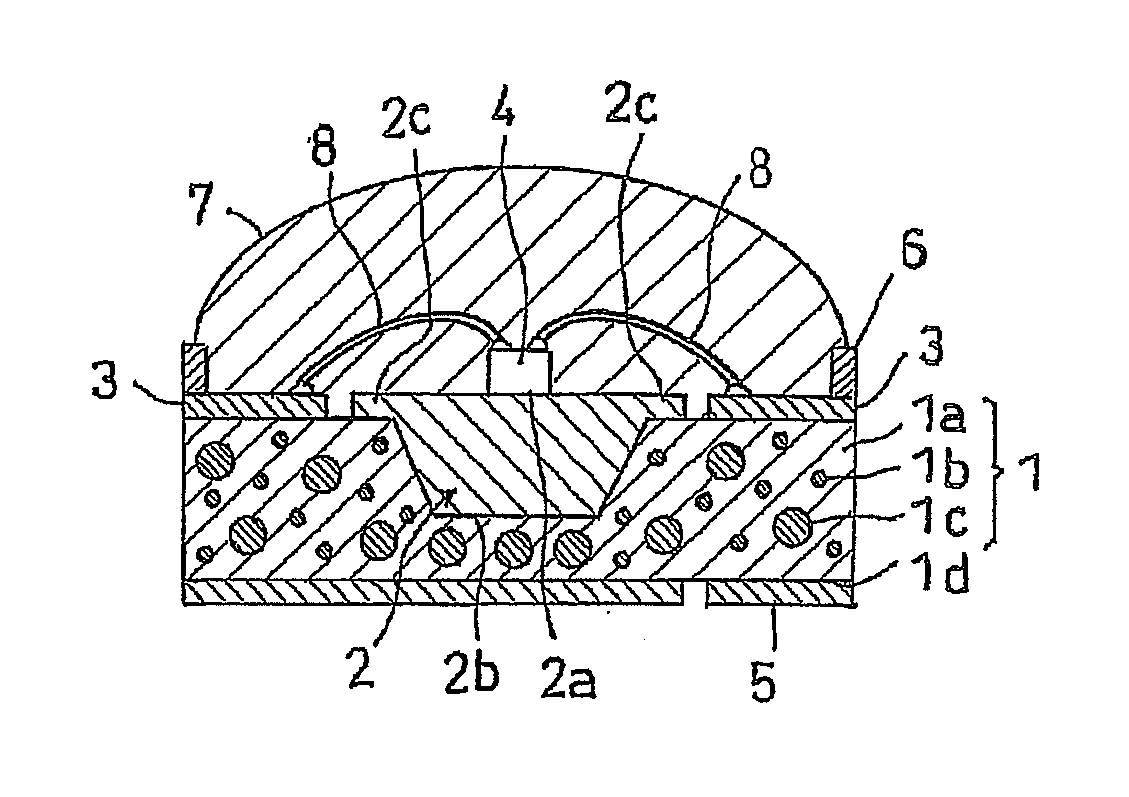
[0031]Hereafter, embodiments of the present invention will be described with reference to the drawings. FIG. 1 is a cross-sectional view showing one example of a substrate for a light emitting element package of the present invention, showing a state in which a light emitting element is mounted and packaged.

[0032]As shown in FIG. 1, the substrate for a light emitting element package of the present invention includes an insulating layer 1 composed of a resin 1a containing heat conductive fillers 1b, 1c; a thick metal section 2 formed under a mounting position of a light emitting element 4; and a surface electrode section 3 formed on a mounting side of the insulating layer 1 separately from the thick metal section 2.

[0033]In the present embodiment, an example is shown in which the mounting surface 2a of the thick metal section 2 for mounting the light emitting element 4 is exposed; the thick metal section 2 is formed to be thick from the mounting surface 2a towards the back surface of...


PUM


Abstract

This invention provides a substrate for a light emitting element package that can obtain a sufficient heat dissipation effect from a light emitting element and can also lower the costs and reduce the size as a substrate for packaging the light emitting element, as well as a light emitting element package using the same. The substrate for a light emitting element package includes an insulating layer 1 composed of a resin 1a containing heat conductive fillers 1b, 1c, a thick metal section 2 formed under a mounting position of a light emitting element 4, and a surface electrode section 3 formed on a mounting side of said insulating layer 1 separately from said thick metal section 2.

Description

TECHNICAL FIELD[0001]The present invention relates to a substrate for a light emitting element package used in packaging a light emitting element such as a LED chip, as well as to a light emitting element package using the same.BACKGROUND ART[0002]In recent years, as illuminating and light-emitting means that can reduce the weight and thickness and can save electric power consumption, a light emitting diode has been attracting people's attention. As a mode of mounting a light emitting diode, there are known a method of mounting a bare chip (LED chip) of a light emitting diode directly on a circuit board and a method of packaging a LED chip by bonding on a small substrate so that the LED chip can be easily mounted on the circuit board and mounting this LED package on the circuit board.[0003]A conventional LED package has a structure such that a LED chip is die-bonded onto a small substrate; the electrode part of the LED chip and the electrode part of the lead are connected with each ...

Claims


Application Information

Patent Timeline
Patent Type & Authority Applications(United States)
IPC IPC(8): H01L33/62
CPCH01L33/486H01L33/641H01L33/642H01L2224/48091H01L2924/01004H01L2924/01012H01L2924/01079H01L2924/01046H01L2924/01057H01L2924/01078H01L2924/00014H01L2924/181H01L2924/00012H01L33/48
Inventor SUZUKI, MOTOHIROYONEMURA, NAOMIMAEDA, TETSUROYOSHIMURA, EIJI
Owner DENKA CO LTD
Why Eureka
Try Eureka