Light emitting diode structure and fabrication method thereof

Inactive Publication Date: 2011-10-27
EVERLIGHT ELECTRONICS
View PDF4 Cites 3 Cited by
  • Summary
  • Abstract
  • Description
  • Claims
  • Application Information

AI Technical Summary

Benefits of technology

[0009]Another aspect of the invention provides a method of fabricating an LED structure, in which the fabrication method can not only fabricate the aforesaid LED structure, the method also has substantially simpler steps.
[0039]Furthermore, when the ohmic contact layer comprises stacked layers of transparent conductive oxides and reflective metals, the overall electrical characteristic and light emitting efficiency of the LED structure are effectively enhanced. Additionally, by designing protruded and recessed portions on the surface of the light emitting device layer and configuring the ohmic contact layer to directly cover the protruded and recessed portions, an contact area of the ohmic contact layer and the light emitting device layer is increased. Accordingly, besides achieving a preferable optical performance, the LED structure may also have an enhanced electrical characteristic. Furthermore, the fabrication method provided by embodiments of the invention fabricates the LED structure having the foregoing advantages by only using a single substrate transfer process. Hence, the fabrication method has substantially simpler steps.

Problems solved by technology

Moreover, conventional vertically oriented LEDs typically require two substrate transfer processes during fabrication.
Therefore, the steps involved in fabricating the conventional vertically oriented LEDs are substantially more complex.

Method used


Image

  • Light emitting diode structure and fabrication method thereof
  • Light emitting diode structure and fabrication method thereof
  • Light emitting diode structure and fabrication method thereof

Examples


first embodiment

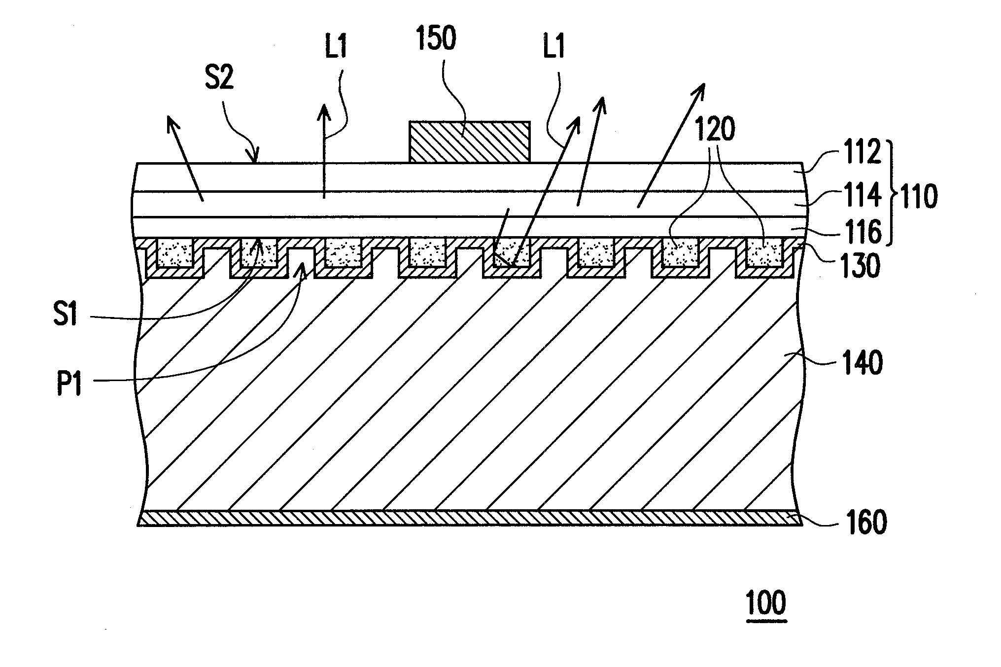
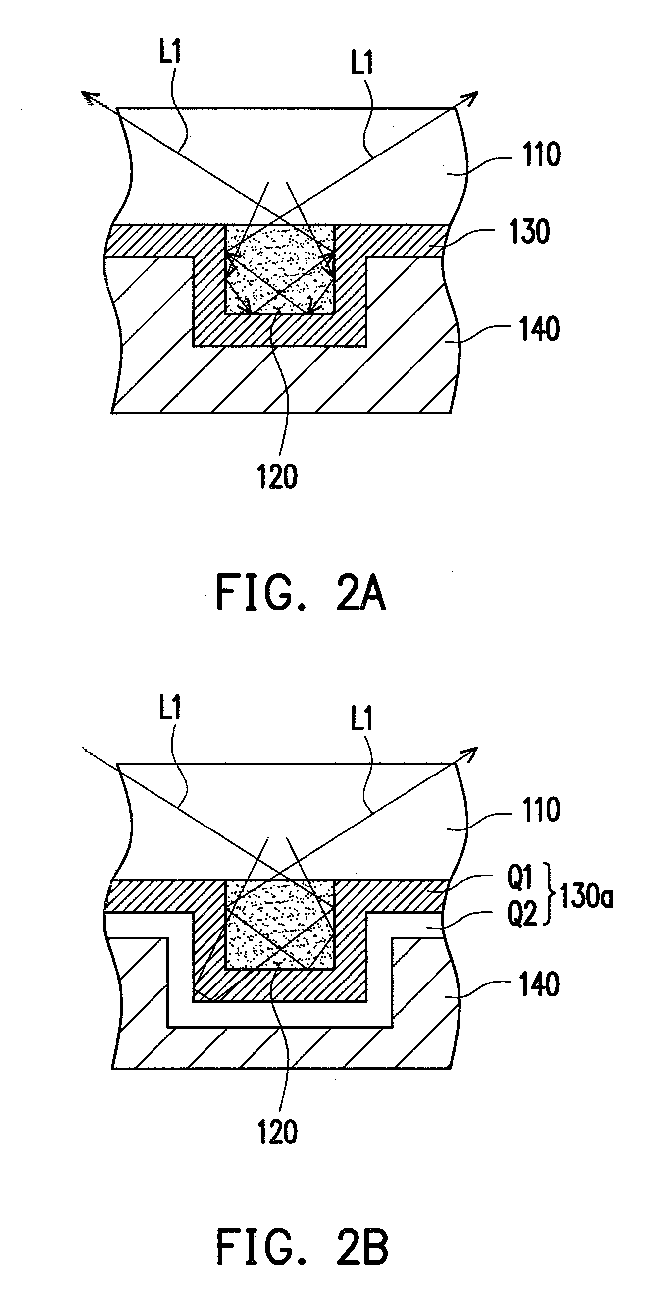
[0051]FIG. 1 is a partial cross-sectional view of a light emitting diode (LED) structure in accordance with a first embodiment of the invention. FIG. 2A is a partial enlarged view of FIG. 1. Referring to FIGS. 1 and 2A, an LED structure 100 according to the present embodiment includes a light emitting device layer 110, a patterned dielectric layer 120, a first ohmic contact layer 130, a conductive layer 140, a first electrode layer 150, and a second electrode layer 160. The light emitting device layer 110 has a first surface S1 and a second surface S2. In the present embodiment, the light emitting device layer 110 includes a first type semiconductor layer 112, a light emitting layer 114, and a second type semiconductor layer 116. The light emitting layer 114 is disposed between the first type semiconductor layer 112 and the second type semiconductor layer 116. More specifically, the first type semiconductor layer 112 is exemplarily a N-type semiconductor layer, the second type semic...

second embodiment

[0076]FIG. 5 is a partial cross-sectional view of an LED structure in accordance with a second embodiment of the invention. Referring to FIG. 5, an LED structure 400 according to the present embodiment includes a light emitting device layer 410, an ohmic contact layer 420, a conductive layer 430, a first electrode layer 440, and a second electrode layer 450. The light emitting device layer 410 has a first surface S1, a second surface S2, a plurality of continually disposed protruded portions 410a and a plurality of recessed portions 410b. The protruded portions 410a and the recessed portions 410b are disposed on the first surface S1. In the present embodiment, the protruded portions 410a and the recessed portions 410b disposed on the first surface S1 are patterned according to a photomask pattern design (e.g., an etching process). The pattern formed on the first surface S1 by the protruded portions 410a and the recessed portions 410b may include a structure of a protruded or recesse...


PUM


Abstract

A light emitting diode structure including a light emitting device layer, a patterned dielectric layer, a first ohmic contact layer, a conductive layer, a first electrode layer and a second electrode layer is provided. The light emitting device layer has a first surface and a second surface opposite to the first surface. The patterned dielectric layer disposed on the first surface has a plurality of openings exposing a portion of the light emitting device layer. The first ohmic contact layer is disposed on the patterned dielectric layer and connected with the first light emitting device layer through the openings. The conductive layer is disposed on the first ohmic contact layer. The first electrode layer is disposed on the conductive layer, and the conductive layer is located between the first ohmic contact layer and the second electrode layer. A fabrication method of the light emitting diode structure is also provided.

Description

CROSS-REFERENCE TO RELATED APPLICATION[0001]This application claims the priority benefit of Taiwan application serial no. 99112860, filed Apr. 23, 2010. The entirety of the above-mentioned patent application is hereby incorporated by reference herein and made a part of this specification.BACKGROUND OF THE INVENTION[0002]1. Field of the Invention[0003]The invention relates generally to light emitting diode, and more particularly to a light emitting diode structure.[0004]2. Description of Related Art[0005]Due to advantages of long lifetime, small volume, great resistance to vibration, low heat emission, and low power consumption, light emitting diodes (LEDs) have been extensively applied in various home appliances and indicators or light sources of various instruments.[0006]Typically speaking, high brightness vertically oriented LEDs have an issue of irregular current distribution, as well as a highly directional property in a provided light, in which the high directional property ref...

Claims


Application Information

Patent Timeline
IPC IPC(8): H01L33/38
CPCH01L33/387H01L33/46H01L33/0079H01L33/0093
Inventor LIN, HSIEN-CHIATANG, TZU-YU
Owner EVERLIGHT ELECTRONICS
Why Eureka
Try Eureka