
Vacuumed device and a scanning electron microscope

Active Publication Date: 2011-09-01
B NANO
View PDF25 Cites 24 Cited by
  • Summary
  • Abstract
  • Description
  • Claims
  • Application Information

AI Technical Summary

Benefits of technology

[0015]A method for maintaining a scanning electron microscope, the method includes: replacing a first vacuumed device by a second vacuumed device, wherei

Problems solved by technology

The replacement process is time consuming and also requires designing the SEM to be large enough to allow the disassembly of these components.
This process is time consuming and requires expertise.
For example, the entire cycle of replacing a Schottky emitter and bringing the system to full operational mode can take more than 12 hours.

Method used


Image

  • Vacuumed device and a scanning electron microscope
  • Vacuumed device and a scanning electron microscope
  • Vacuumed device and a scanning electron microscope

Examples


Embodiment Construction

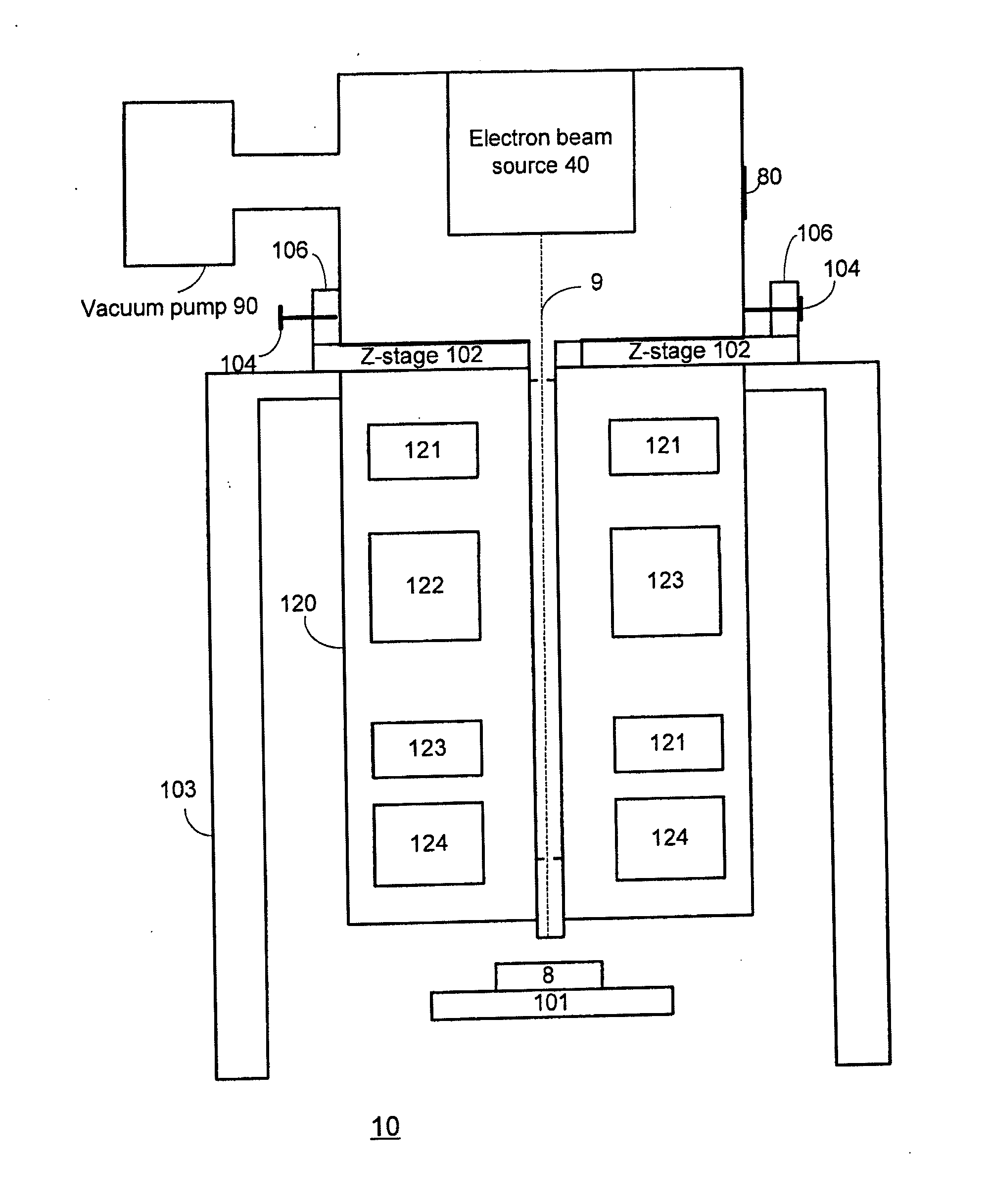
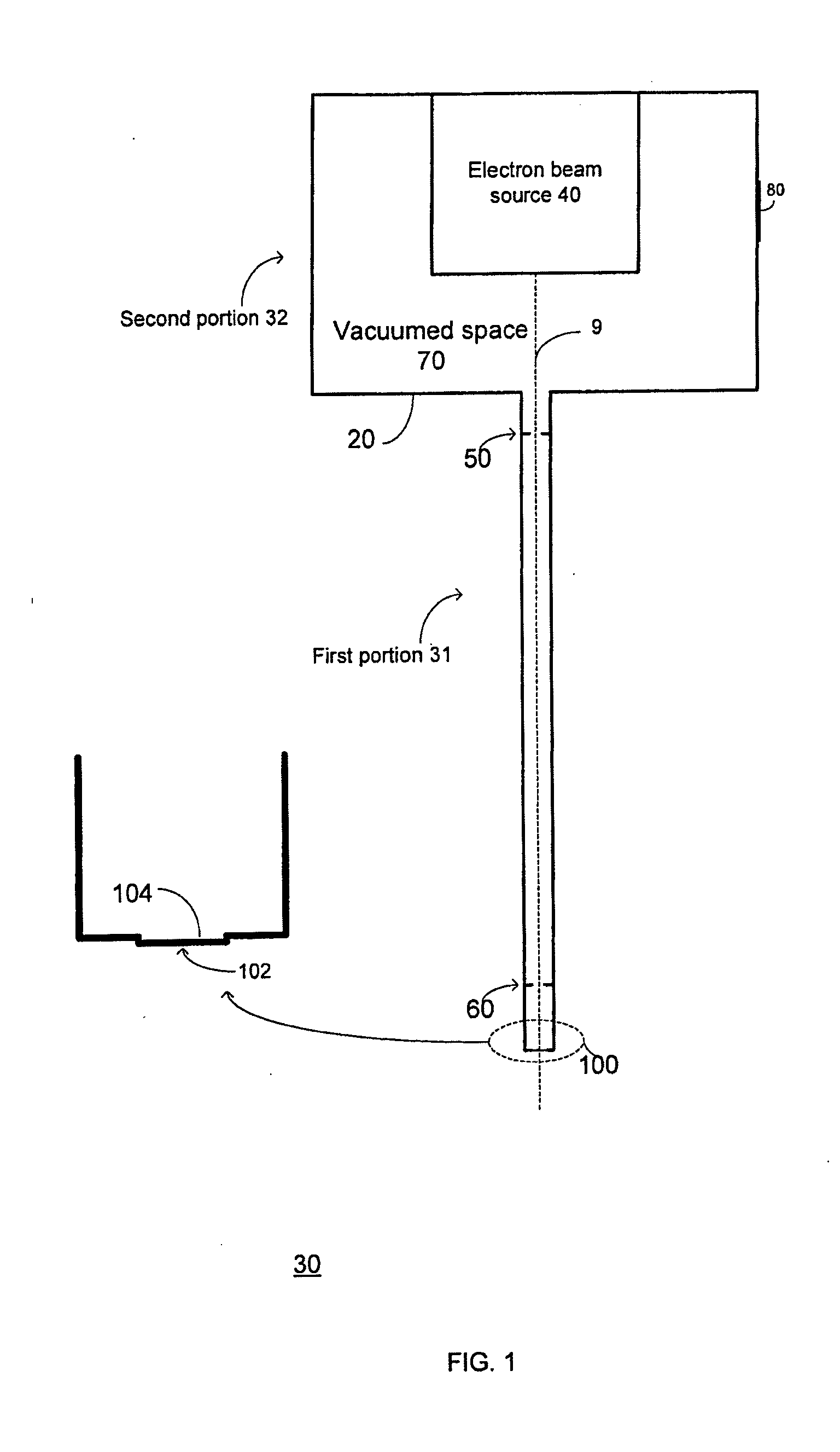
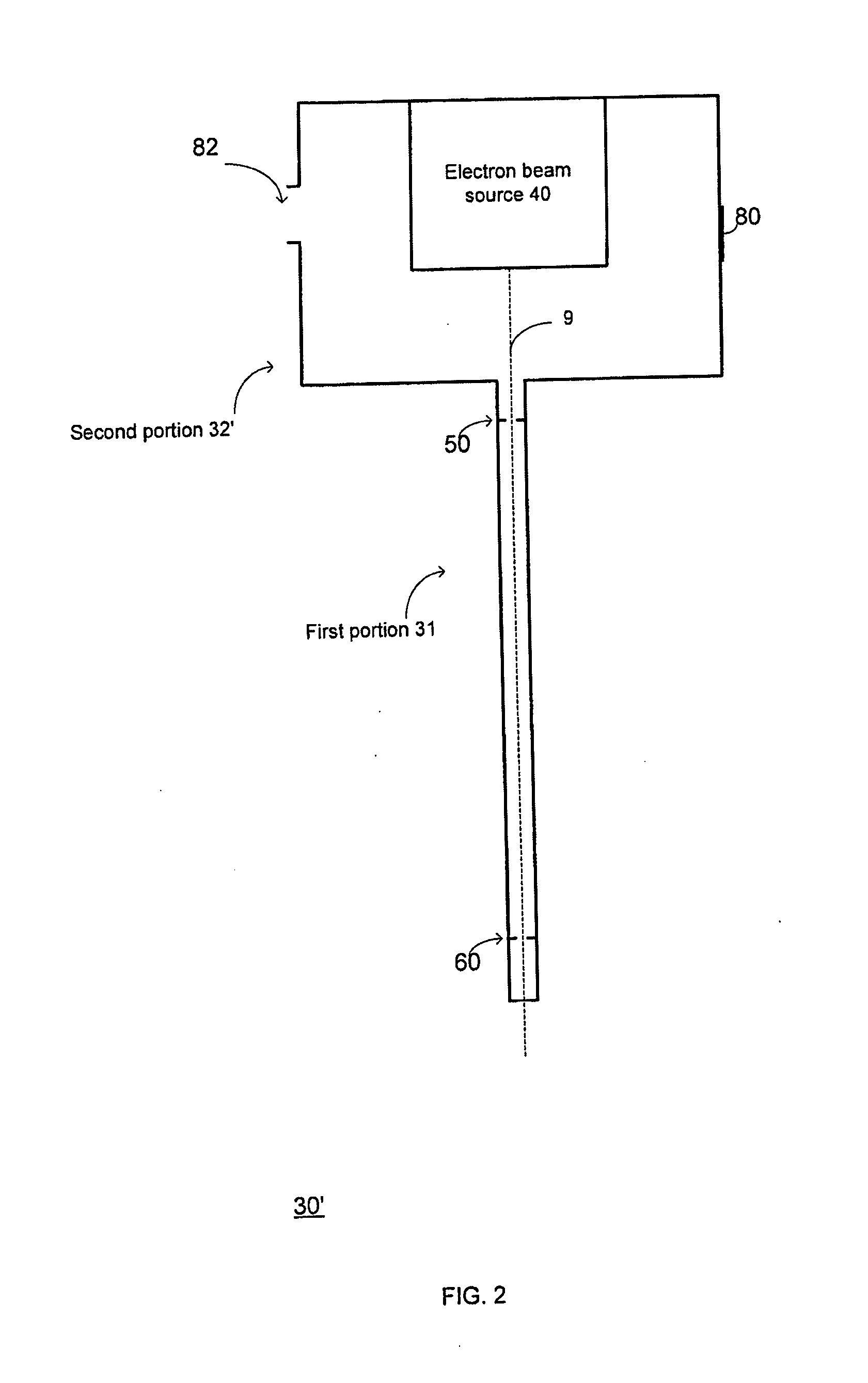
[0030]According to an embodiment of the invention a SEM, an apparatus and a vacuumed device are provided. The SEM may include the apparatus. The apparatus may include the vacuumed device. The vacuumed device is also referred to as a replaceable vacuumed device.

[0031]According to various embodiments of the invention the SEM obtains images of an object that is located in a non-vacuumed environment. The SEM includes one or more non-vacuumed components and the vacuumed device (or the apparatus). A non-vacuumed component is a component that is not located in a vacuumed environment.

[0032]Vacuum is maintained in the vacuumed device but conveniently is not maintained in other portions of the SEM. If the vacuumed device malfunctions the entire vacuumed device is replaced. The vacuumed device is relatively small and the vacuum within the vacuumed device can be maintained quite easily by using a low throughput vacuum pump.

[0033]The vacuumed device is replaceable by its entirety, it is sealed a...


PUM

PropertyMeasurementUnit
Diameteraaaaaaaaaa
Diameteraaaaaaaaaa
Volumeaaaaaaaaaa

Abstract

A vacuumed device that includes: a sealed housing, an electron beam source, an electron optic component, a thin membrane, and a detector. The thin membrane seals an aperture of the sealed housing. The sealed housing defines a vacuumed space in which vacuum is maintained. The electron beam source is configured to generate an electron beam that propagates within the vacuumed space, interacts with the electron optic component and passes through the thin membrane. A first portion of the sealed housing is shaped to fit a space defined by non-vacuumed scanning electron microscope components that are maintained in a non-vacuum environment.

Description

RELATED APPLICATIONS[0001]This application claims priority of U.S. provisional patent Ser. No. 61 / 100,735, filing date 28 Sep. 2008, which is incorporated herein by reference.BACKGROUND OF THE INVENTION[0002]High resolution microscopy is used in research and development, quality assurance and production in diverse fields such as material science, life science, the semiconductor industry and the food industry.[0003]Optical microscopy dating back to the seventeenth century, has reached a brick wall, defined by the wavelength of deep Ultra Violet photons, giving a finest resolution of about 80 nm.[0004]The popularity of optical microscopy stems from its relative low price, ease of use and the variety of imaging environment all translated to availability.[0005]A scanning electron microscope (SEM) provides a much finer resolution (down to a few nanometers) but in order to achieve that high resolution the inspected object should be placed in a vacuum environment and be scanned by an elect...

Claims


Application Information

Patent Timeline
IPC IPC(8): H01J37/28H01J3/14H01J3/26B23P6/00
CPCH01J37/16H01J37/18Y10T29/4973H01J2237/0245H01J2237/164H01J37/28
Inventor SHACHAL, DOVDE PICCIOTTO, RAFI
Owner B NANO
Learn More