4d device process and structure

a technology of 4d devices and process steps, applied in the field of microelectronics, can solve the problems of increasing access time (or slowing speed), difficult to supply power to the stacked system stack, and typically difficult to solve the cooling of the system, and achieve the effect of high density memory

Inactive Publication Date: 2011-07-14
IBM CORP
View PDF16 Cites 51 Cited by
  • Summary
  • Abstract
  • Description
  • Claims
  • Application Information

AI Technical Summary

Problems solved by technology

In a 2D configuration more and more device contents have to be placed outside this area and more clock-cycles are needed to access them, and as a result, increases access time (or slowers speed).
Aso, it is difficult to supply power to the stacked system stack.
In all 3DI integration schemes mentioned above, the cooling of the system is typically a difficult issue to resolve.
Some work in micro-channels cooling for 3DI only limits the cooling through surface layer and is difficult to achieve an effective cooling with more stacks involved in the 3D systems.
One particular issue associated with 3DI through-Si connections comprises the ESD (electro-static discharge) protection load.
This can be a large load as the number of devices increase and requires a large driver to access the 3DI circuits which could significantly slow them down.
This limits the number of 3DI devices as the heat dissipation become a road block for further 3D content increase.
These prior art devices and methods of assembling and using them have proved successful, however, they also present several issues, such as for example in chip stacking, edge connection leads to signal delay, lower I / O density, difficulties in powering the system and difficulties in cooling the system in high power applications.
Similarly, the current through-Si 3D wafer stacking processes and resultant devices present issues, e.g., thin Si construction (20 um) requires stacking wafers one at a time to allow through-Si vias; it is difficult to make the via less than 5 um in size and 10 um in pitch in devices employing Cu; through-Si vias can be made from W but W has a higher resistivity than Cu; through-vias pass through the bonding interface making bonding defects difficult to control; wafer stacks are limited due to bonding thermal cycles; the process is complex and introduces via yield and wafer yield issues; manufacturing involves long process cycles; wafer level distortions are introduced; it is difficult to cool the system; and it is difficult to dissipate power.

Method used


Image

  • 4d device process and structure
  • 4d device process and structure
  • 4d device process and structure

Examples


Embodiment Construction

[0049]To achieve these and other advantages, and in accordance with the purpose of this invention as embodied and broadly described herein, the following detailed embodiments comprise disclosed examples that can be embodied in various forms.

[0050]The specific processes compounds, compositions, and structural details set out herein not only comprise a basis for the claims and a basis for teaching one skilled in the art to employ the present invention in any novel and useful way, but also provide a description of how to make and use this invention.

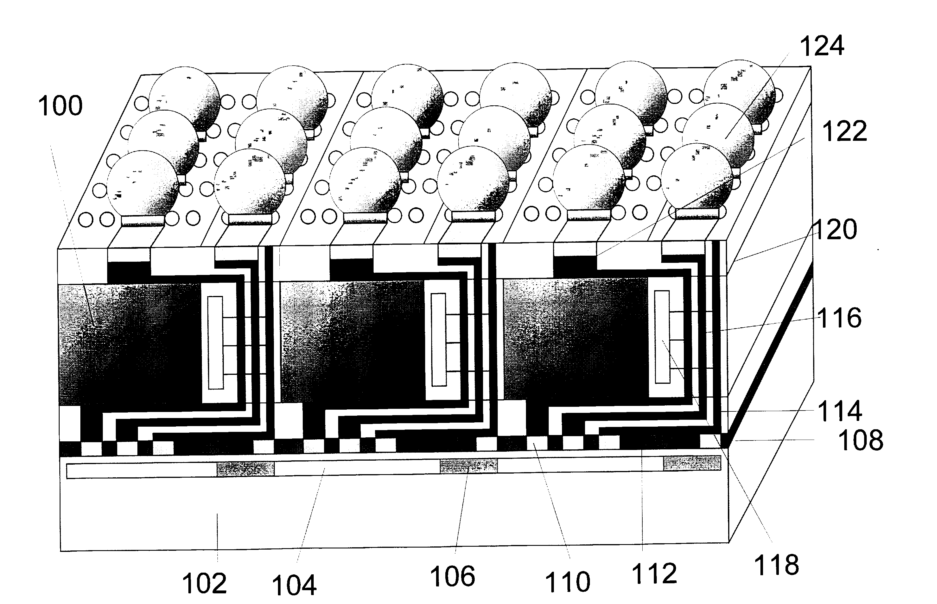
[0051]More specifically, the following written description, claims, and attached drawings set out the present invention which comprises a new 4DI system that increases system density within the 1 clock-cycle up to about 100× more in memory density than the 2D system, as well as a process for making the system. In addition to memory density increase the 4DI also provides a micro-channel cooling capability for the system. The I / O density can s...


PUM


Abstract

a 4D device comprises a 2D multi-core logic and a 3D memory stack connected through the memory stack sidewall using a fine pitch T&J connection. The 3D memory in the stack is thinned from the original wafer thickness to no remaining Si. A tounge and groove device at the memory wafer top and bottom surfaces allows an accurate stack alignment. The memory stack also has micro-channels on the backside to allow fluid cooling. The memory stack is further diced at the fixed clock-cycle distance and is flipped on its side and re-assembled on to a template into a pseudo-wafer format. The top side wall of the assembly is polished and built with BEOL to fan-out and use the T&J fine pitch connection to join to the 2D logic wafer. The other side of the memory stack is polished, fanned-out, and bumped with C4 solder. The invention also comprises a process for manufacturing the device. In another aspect, the invention comprises a 4D process and device for over 50× greter than 2D memory density per die and an ultra high density memory.

Description

FIELD OF THE INVENTION[0001]This invention relates to microelectronics comprising, inter glia, electronic device integration devices and processes in 3D system integration, and a 4D higher level system integration than the 3D integration. In one aspect, the invention comprises a 4D process and device for 50 stacks (50×) per die and an ultra high density memory.BACKGROUND OF THE INVENTION AND RELATED ART[0002]3D integration (3DI) comprises a device system integration method that brings heterogeneous devices together in close proximity so that they function as a homogeneous device. 3DI is different than traditional 2D planar back-end-of-line (BEOL) integration in that 3DI adds an additional dimension, (Z) integration, which not only allows more devices from different sources and types to be integrated into the system in close proximilty, but also enables them to function as a unit.[0003]This integration allows more device content (more memories) and faster access times (shorter distan...

Claims


Application Information

Patent Timeline
Patent Type & Authority Applications(United States)
IPC IPC(8): H05K7/20H01L21/78H01L21/306H01L21/66H05K1/14H05K1/11B32B37/02
CPCB32B37/02H01L2924/1461B32B38/1841B32B2309/105B32B2310/0843B32B2457/14H01L23/473H01L24/96H01L25/0652H01L25/0657H01L25/18H01L25/50H01L2225/06513H01L2225/06541H01L2225/06551H01L2225/06555H01L2225/06572H01L2225/06589H01L2225/06593H01L2924/01013H01L2924/01029H01L2924/01077H01L2924/01078H01L2924/01079H01L2924/01082H01L2924/10329H01L2924/01005H01L2924/01006H01L2924/01019H01L2924/01023H01L2924/01033H01L2924/01074H01L2924/01075H01L2924/01076H01L2924/014H01L24/94H01L2224/94H01L2924/15153B32B37/12H01L2224/06181H01L2224/32145H01L2224/16147H01L2224/83005H01L2224/26135H01L24/81H01L24/83H01L24/92H01L24/97H01L29/0657H01L2224/13147H01L2224/291H01L2224/2919H01L2224/73253H01L2224/81191H01L2224/8314H01L2224/9202H01L2224/96H01L2224/97H01L2224/83141H01L2224/0401H01L2224/83H01L2924/00014H01L2224/03H01L2224/11H01L2224/81H01L2924/00H01L23/49827H01L23/481H01L24/09H01L24/32H01L2224/05144H01L2224/05147H01L2224/08145H01L2224/29147H01L2225/06544H01L2225/06562H01L2924/1032H01L2924/1204H01L2924/1431H01L2924/1434
Inventor HAENSCH, WILFRIEDYU, ROY R.
Owner IBM CORP
Why Eureka
Try Eureka