Semiconductor memory device and method for operating the same

Inactive Publication Date: 2011-06-30
SK HYNIX INC
View PDF6 Cites 7 Cited by
  • Summary
  • Abstract
  • Description
  • Claims
  • Application Information

AI Technical Summary

Benefits of technology

[0011]Exemplary embodiments of the present invention are directed to a semiconductor memory device in which the input numbers of an auto-refresh command are less than the counting numbers of an internal address, thereby minimizing the magnitude of electric current consumed for an auto-refresh operation.

Problems solved by technology

Due to a memory cell structure of a semiconductor memory device configured with a capacitor, if the refresh operation is not carried out, a memory cell loses data due to a leakage current.
Furthermore, a larger amount of electric current is consumed in order to count the internal addresses IN_ADDRESS having a large number of bits.

Method used


Image

  • Semiconductor memory device and method for operating the same
  • Semiconductor memory device and method for operating the same
  • Semiconductor memory device and method for operating the same

Examples


Embodiment Construction

[0019]Exemplary embodiments of the present invention will be described below in more detail with reference to the accompanying drawings. The present invention may, however, be embodied in different forms and should not be construed as limited to the embodiments set forth herein. Rather, these embodiments are provided so that this disclosure will be thorough and complete, and will fully convey the scope of the present invention to those skilled in the art. Throughout the disclosure, like reference numerals refer to like parts throughout the various figures and embodiments of the present invention.

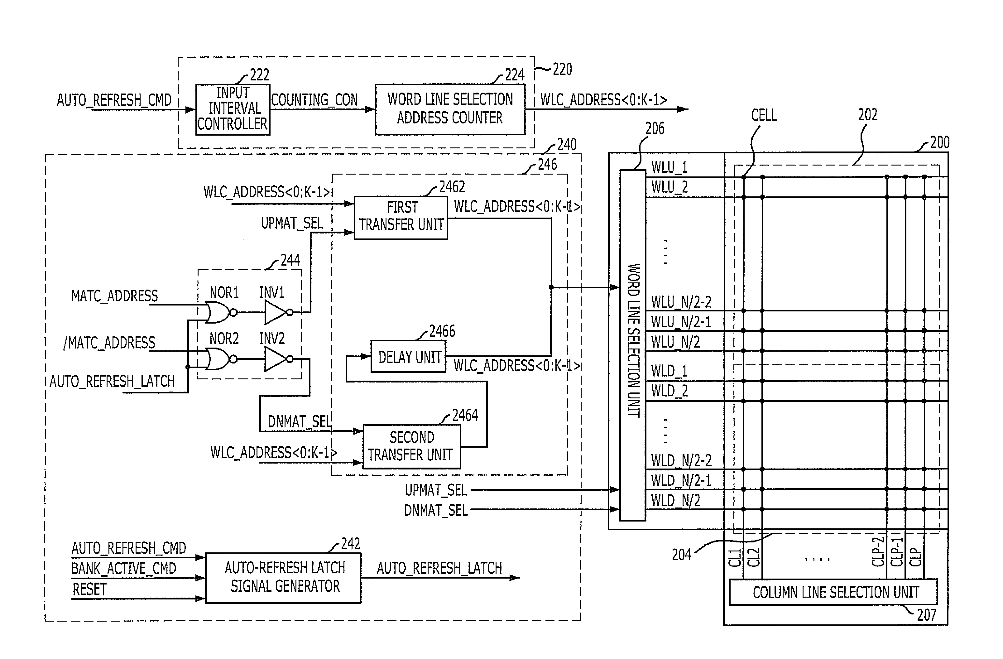
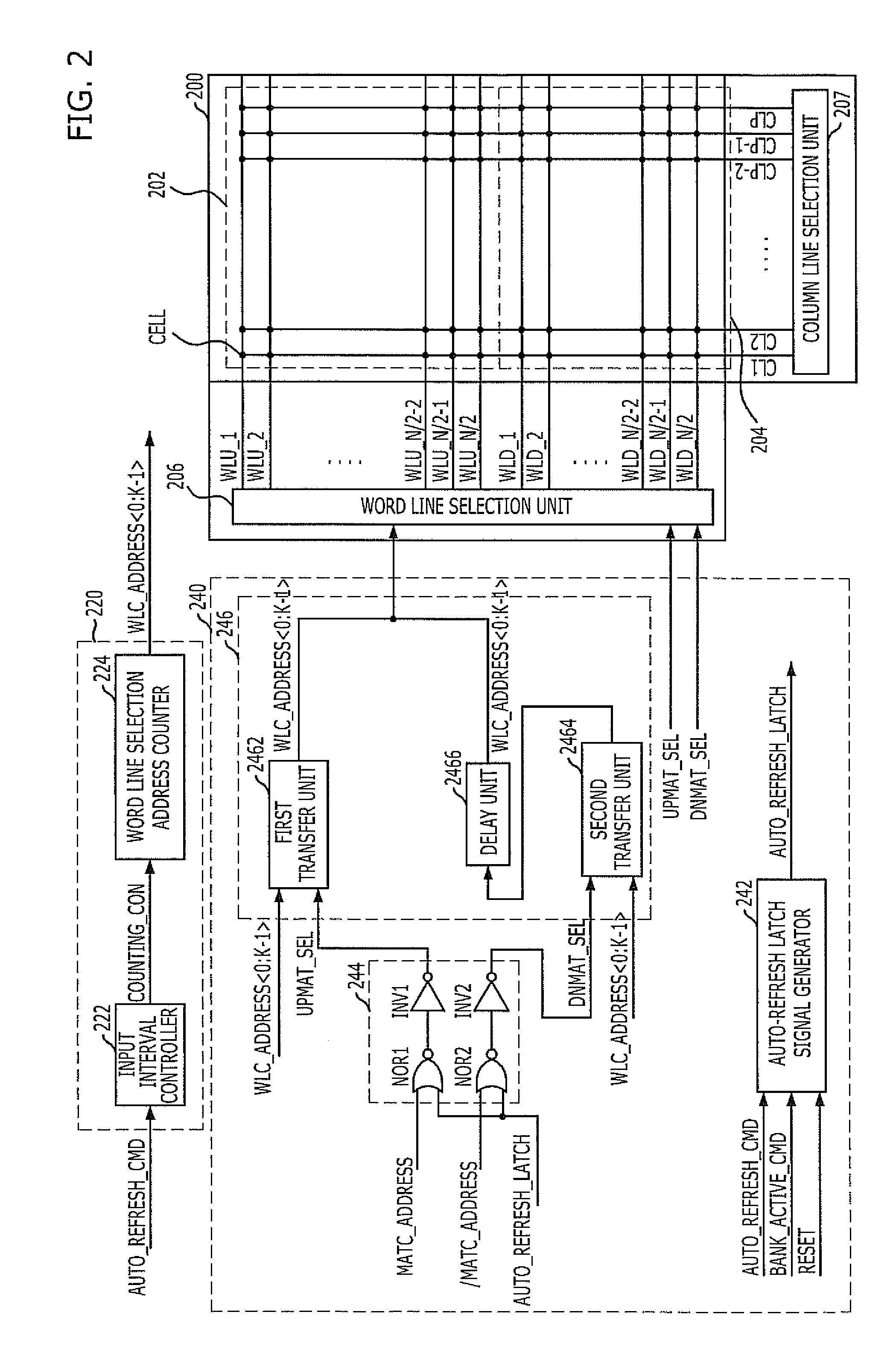
[0020]FIG. 2 is a block diagram of an auto-refresh circuit of a semiconductor memory device in accordance with an embodiment of the present invention.

[0021]Referring to FIG. 2, the auto-refresh circuit of the semiconductor memory device in accordance with the embodiment of the present invention includes a bank 200, an address counting unit 220, and an address transferring unit 240. The bank ...


PUM


Abstract

A semiconductor memory device includes a bank having a plurality of mats, an address counting unit configured to receive an auto-refresh command consecutively applied at predetermined intervals corresponding to a number of the mats, and sequentially count an internal address in response to the auto-refresh command, and an address transferring unit configured to enable the plurality of mats in response to the auto-refresh command, and transfer the internal address to the plurality of mats at predetermined time intervals.

Description

CROSS-REFERENCE TO RELATED APPLICATION[0001]The present application claims priority of Korean Patent Application No. 10-2009-0133001, filed on Dec. 29, 2009, which is incorporated herein by reference in its entirety.BACKGROUND OF THE INVENTION[0002]Exemplary embodiments of the present invention relate to a semiconductor design technology, and more particularly, to an auto-refresh operation of a semiconductor memory device.[0003]Generally, a semiconductor memory device is required to perform a refresh operation in order to retain data stored in a memory cell. A refresh operation is an operation of reading data stored in a memory cell, amplifying the read data, and again storing data in the corresponding memory cell. Due to a memory cell structure of a semiconductor memory device configured with a capacitor, if the refresh operation is not carried out, a memory cell loses data due to a leakage current. Hence, the refresh operation must be carried out.[0004]The refresh operation is per...

Claims


Application Information

Patent Timeline
IPC IPC(8): G11C7/00G11C8/00G11C8/08
CPCG11C11/406G11C11/40618G11C11/40611G11C8/04G11C11/408G11C2211/4065
Inventor KIM, DAE-SUKLEE, JONG-CHERN
Owner SK HYNIX INC
Why Eureka
Try Eureka