Shell and display module of mobile communication terminal and a method of forming the same
- Summary
- Abstract
- Description
- Claims
- Application Information
AI Technical Summary
Benefits of technology
Problems solved by technology
Method used
Image
Examples
example 1
[0034](1) First, said shell body 12 was made with transparent or semitransparent materials by injection or molding, said materials can be one or more selected from polycarbonate whose weight average molecular weight is about 20,000-100,000, polymethyl methacrylate (PMMA) whose weight average molecular weight is about 25,000-200,000, silicone (RUBBER) whose weight average molecular weight is about 120,000-200,000, polyethylene terephthalate (PET) whose weight average molecular weight is about 20,000-50,000; secondly, said shell body 1 was cleaned with ultrasonic in order to clean the besmirch and impurity on the outer surface 121 of said shell body 12, this process was helpful to vapor deposition; then, is said outer surface 121 was sprayed a primer layer with thickness of 10 um using spray coating; finally, said coated outer surface 121 was dried on automatic spraying line.
[0035](2) Said shell body 12 was put into a metal vapor coating furnace for physical vapor deposition, and Sn w...
example 2
[0038](1) According to the technology for forming mobile phone shell in the present disclosure, said shell body 12 was formed with transparent or semitransparent materials using molding, said materials can be one or more materials selected from the materials referred in example 1; said shell body 1 was cleaned with ultrasonic wave in order to clean the besmirch and impurity on the outer surface 121 of said shell body 12, this process was helpful to vapor deposition; then, said outer surface 121 was sprayed a primer layer with thickness of 30 um using spray coating; then, said coated outer surface 121 was dried on automatic spraying line.
[0039](2) Said shell body 12 was put into a metal vapor coating furnace for physical vapor deposition, and Sn was used as target material. The mount of Sn was 0.1 g per target, there were 32 targets used for spraying the outer surface 121 which was sprayed primer layer. The amount of Sn was determined by the transmittance of said shell. In the presen...
example 1 ′
Example 1′
[0058]The embodiment illustrates a forming method of the mobile phone shell 1 and an assembly method of the display module.
[0059]First, a semitransparent-semireflecting layer 11 was formed on the shell 1 by PVD technology to provide mirror or semi-mirror effects. According to the embodiments of the present disclosure, the transmittance of the semitransparent-semireflecting layer 11 was controlled in about 5%-20%, further, the transmittance was controlled in about 5%-15%.
[0060]Second, the patterns 13 were printed on the inner surface of the shell 1 by thermal transfer printing.
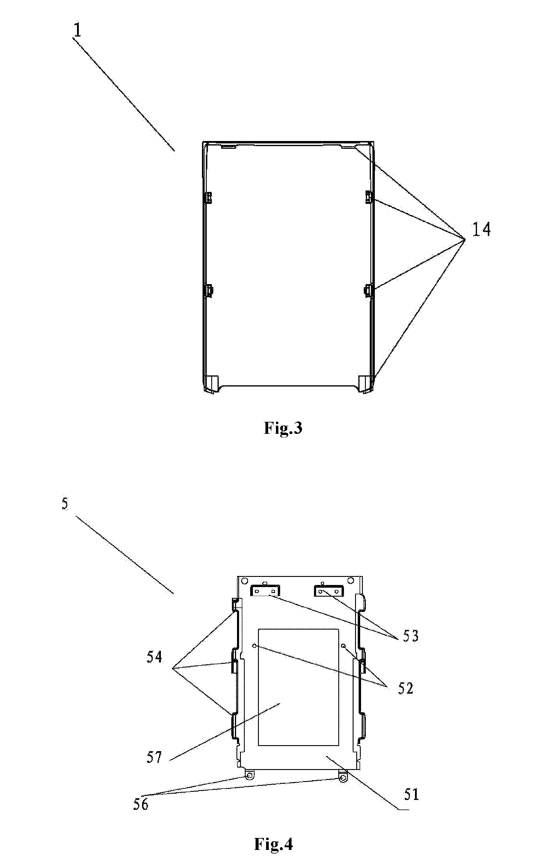
[0061]Third, the localizing frame 5 was formed by punching formed stainless steel, and the LED 3 was adhered in the LED containing part in the localizing frame 5 with adhesive, such as transparent strong optical adhesive and so on.
[0062]Fourth, the localizing hole 22 was punched in the light guide plate 2, and adhesive was coated on it, such as transparent strong optical adhesive said above.
[0063]Fift...
PUM
| Property | Measurement | Unit |
|---|---|---|
| Thickness | aaaaa | aaaaa |
| Molecular weight | aaaaa | aaaaa |
| Transparency | aaaaa | aaaaa |
Abstract
Description
Claims
Application Information
 - R&D
- Intellectual Property
- Life Sciences
- Materials
- Tech Scout
- Unparalleled Data Quality
- Higher Quality Content
- 60% Fewer Hallucinations
Browse by: Latest US Patents, China's latest patents, Technical Efficacy Thesaurus, Application Domain, Technology Topic, Popular Technical Reports.
© 2025 PatSnap. All rights reserved.Legal|Privacy policy|Modern Slavery Act Transparency Statement|Sitemap|About US| Contact US: help@patsnap.com


