
Multi-stack package LED

a technology of led package and led light, applied in the direction of basic electric elements, electrical apparatus, semiconductor devices, etc., can solve the problems of poor excitation effect of fluorescent powder, achieve better light emission efficiency, reduce secondary excitation loss, and improve color rendering

Inactive Publication Date: 2011-06-30
IND TECH RES INST
View PDF3 Cites 43 Cited by
  • Summary
  • Abstract
  • Description
  • Claims
  • Application Information

AI Technical Summary

Benefits of technology

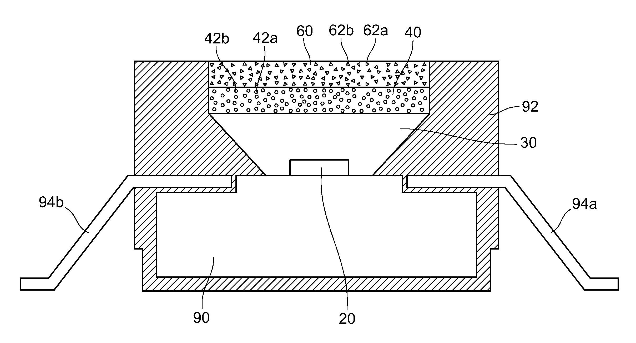
[0011]In view of the above problems, the present disclosure provides a multi-stack package LED, which can eliminate the phenomena of secondary excitation between different kinds of fluorescent powders, thereby avoiding the loss of the light emission efficiency caused by the secondary excitation and reducing the loss in absorption and conversion.
[0021]The wavelengths of the fluorescent powder layers are designed according to the stack relations, and the optical bandpass filter layers filter and reflect the wavelengths, so that the excitation light generated after the fluorescent powder layers are excited will not be absorbed by other fluorescent powder layers, thereby eliminating the loss of the secondary excitation and achieve a better light emission efficiency. Then, after appropriately adjusting the wavelengths of the excitation lights of all fluorescent powder layers and the wavelength of the LED light emitted by the LED, a mixed light having high color rendering property is obtained.

Problems solved by technology

Although this technology may generate the white light, the excitation effect of the fluorescent powder is not good and the light emission efficiency is a half of an ordinary white LED.

Method used


Image

  • Multi-stack package LED
  • Multi-stack package LED
  • Multi-stack package LED

Examples


first embodiment

The First Embodiment

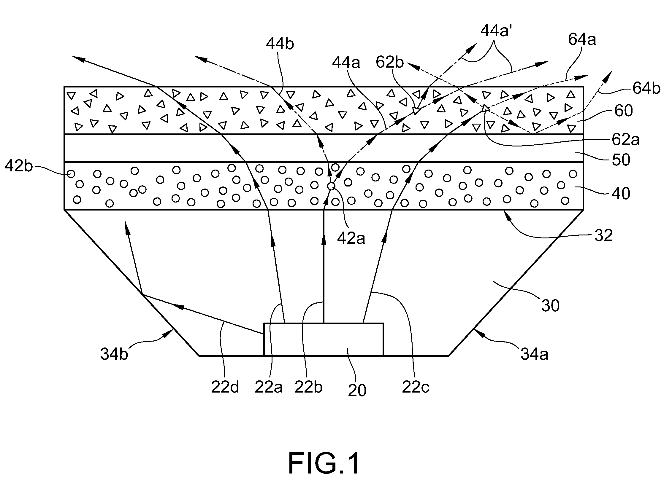
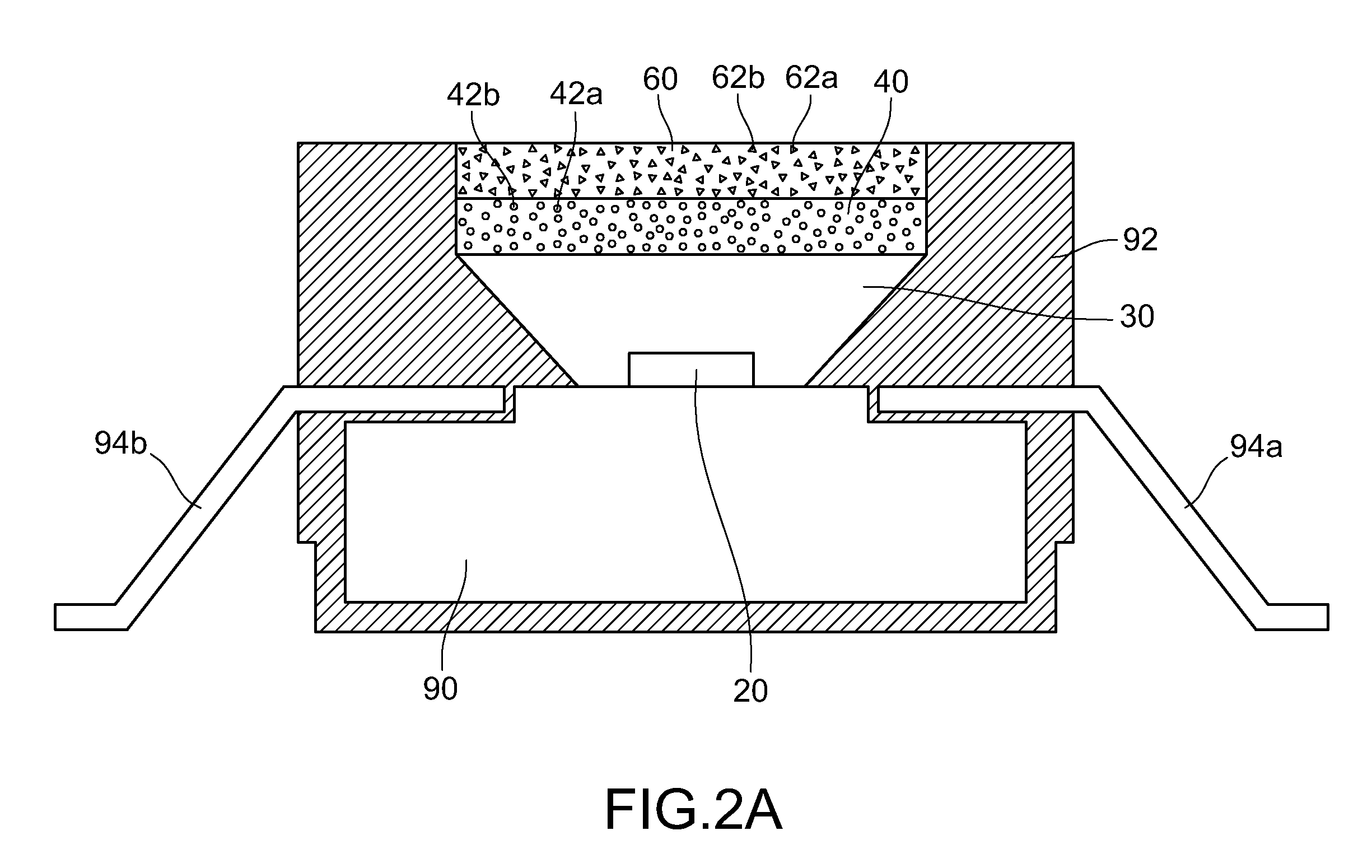
[0034]Firstly, FIG. 1 is a schematic sectional view of a multi-stack package LED according to the present disclosure. Referring to FIG. 1, the multi-stack package LED comprises an LED chip 20, a package 30, a first fluorescent powder layer 40, a first optical bandpass filter layer 50 and a second fluorescent powder layer 60.

[0035]The LED chip 20 generates LED lights 22a, 22b, 22c, 22d when being driven (indicated by thin solid lines in the figure). The LED lights 22a, 22b, 22c, 22d generated by the LED chip 20 may be UV lights, blue lights or green lights. The wavelengths of the LED lights 22a, 22b, 22c, 22d may fit the corresponding wavelengths of the first fluorescent powder layer 40, the first optical bandpass filter layer 50 and the second fluorescent powder layer 60 and are mixed, and the mixed light may be, but is not limited to, a white light.

[0036]The package 30 is covered on the LED chip 20. A surface of the package 30 opposite to the LED chip 20 is a li...

second embodiment

The Second Embodiment

[0057]Then, FIG. 3 is a schematic sectional view of a multi-stack package LED according to the second embodiment of the present disclosure. Referring to FIG. 3, the multi-stack package LED comprises multiple LED chips 20a, 20b, a package 30, a first fluorescent powder layer 40, a first optical bandpass filter layer 50, a second fluorescent powder layer 60, a second optical bandpass filter layer 70 and a third fluorescent powder layer 80.

[0058]The light LED chips 20a, 20b generate the LED light when being driven (the reference numerals of the LED light, the first excitation light and the second excitation light are the same as those of FIG. 1, to simplify the drawings and the description, the reference numerals thereof are omitted in the second embodiment and the third embodiment and the following descriptions). The number of the LED chips 20a, 20b is, but not limited to, two in this embodiment, and one or more than two LED chips may be disposed.

[0059]The package...

third embodiment

The Third Embodiment

[0065]FIG. 4 is a schematic sectional view of a multi-stack package LED according to a third embodiment of the present disclosure. Referring to FIG. 4, the multi-stack package LED comprises LED chips 20a, 20b, a package 30, a first fluorescent powder layer 40, a second fluorescent powder layer 60 and a third fluorescent powder layer 80.

[0066]The first fluorescent powder layer 40 has multiple first fluorescent powders 42a, 42b. The second fluorescent powder layer 60 has multiple second fluorescent powders 62a, 62b. The third fluorescent powder layer 80 has multiple third fluorescent powders 82a, 82b. When the first fluorescent powders 42a, 42b are excited, the first excitation light is generated. When the second fluorescent powders 62a, 62b are excited, the second excitation light is generated. When the third fluorescent powders 82a, 82b are excited, the third excitation light is generated.

[0067]The refraction index of the third fluorescent powder layer 80 is high...


PUM

PropertyMeasurementUnit
central wavelengthaaaaaaaaaa

Abstract

A multi-stack package light emitting diode (LED) includes an LED chip, a first fluorescent powder layer, a first optical bandpass filter layer and a second fluorescent powder layer. The LED chip generates an LED light. The first fluorescent powder layer and the second fluorescent powder layer respectively have a first fluorescent powder and a second fluorescent powder. The first fluorescent powder and the second fluorescent powder are excited by the LED light to respectively generate a first excitation light and a second excitation light. The first optical bandpass filter layer allows the LED light and the first excitation light to pass and reflects the second excitation light. A wavelength of the LED light is shorter than a wavelength of the second excitation light. The wavelength of the second excitation light is shorter than a wavelength of the first excitation light. Therefore, the multi-stack package LED improves a light emission efficiency.

Description

CROSS-REFERENCE TO RELATED APPLICATIONS[0001]This non-provisional application claims priority under 35 U.S.C. §119(a) on Patent Application No(s). 098145139 filed in Taiwan, R.O.C. on Dec. 25, 2009 and Patent Application No(s). 099109463 filed in Taiwan, R.O.C. on Mar. 29, 2010, the entire contents of which are hereby incorporated by reference.BACKGROUND[0002]1. Field of Invention[0003]The present disclosure relates to a light emitting diode (LED), and more particularly to a multi-stack package LED.[0004]2. Related Art[0005]With the improvement of the light emission efficiency of a white LED, the white LED has become a new-generation light source attracting more attentions. At present, the light emission efficiency of the white LED ranges from an experimental-scale 249 lm / W (Lumen Per Watt) to the commercial-scale 100 lm / W. The light emission efficiency is still under improvement.[0006]Although the light emission efficiency of the white LED has been improved, in order to make the co...

Claims


Application Information

Patent Timeline
Patent Type & Authority Applications(United States)
IPC IPC(8): H01L33/48
CPCH01L33/44H01L33/46H01L33/507H01L33/504H01L33/50
Inventor CHENG, CHIA SHENLIN, JIAN SHIANCHEN, SHAU YILIN, HSIU JENPENG, YAO CHI
Owner IND TECH RES INST
Learn More