Circuit arrangement of a voltage controlled oscillator

Inactive Publication Date: 2011-06-23
STMICROELECTRONICS SRL
View PDF9 Cites 43 Cited by
  • Summary
  • Abstract
  • Description
  • Claims
  • Application Information

AI Technical Summary

Benefits of technology

[0025]The purpose of the present invention is therefore of providing a circuit of a voltage controlled oscillator that has better performance and lower power consumption with respect to the aforementioned prior art.

Problems solved by technology

In this type of application, the design of the oscillators is made particularly difficult by the high frequency of the synthesised signal, and by the constraints imposed by power consumption.
Indeed, high values of KV jeopardise the performance of phase noise due to the phenomenon of noise conversion AM-PM.
The main drawbacks are that the phase noise is not optimized in the different oscillation frequency sub-bands identified by the capacitors CSW1-CSWN of the first set 4a and of the second set 4b of capacitors, and that there is an oversize in terms of current consumption by the circuit 1 (and thus power consumption).
However, this leads to an increase of the phase noise.
These are what cause there to be limits in terms of phase noise or excessive power consumption due to the reduction of the Q factor of the LC resonator 2.
This however, reduces the tuning range.
Such an issue can be eliminated by using complementary switches, but this leads to a substantial increase of the parasitic capacities thereof.

Method used


Image

  • Circuit arrangement of a voltage controlled oscillator
  • Circuit arrangement of a voltage controlled oscillator
  • Circuit arrangement of a voltage controlled oscillator

Examples


Embodiment Construction

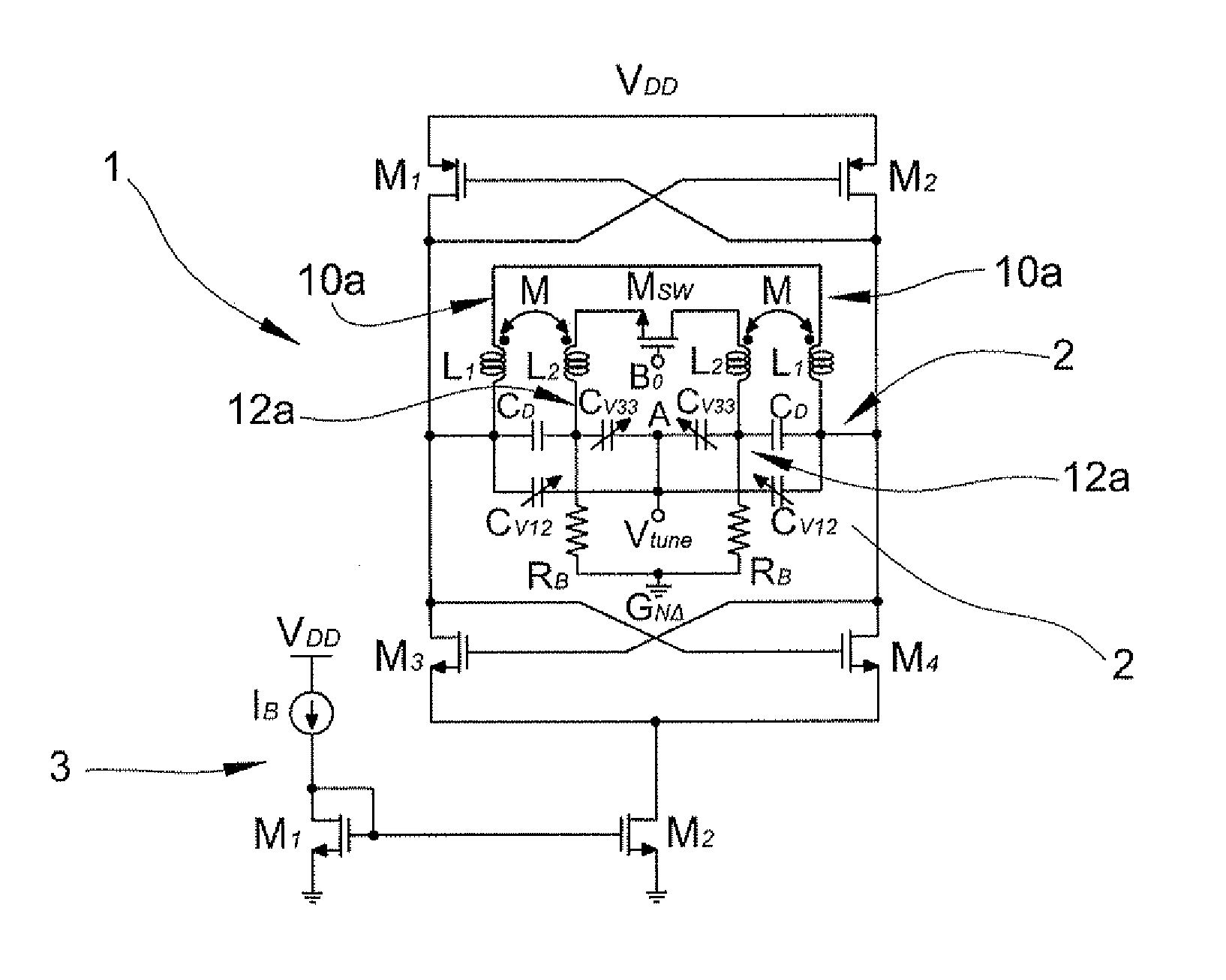
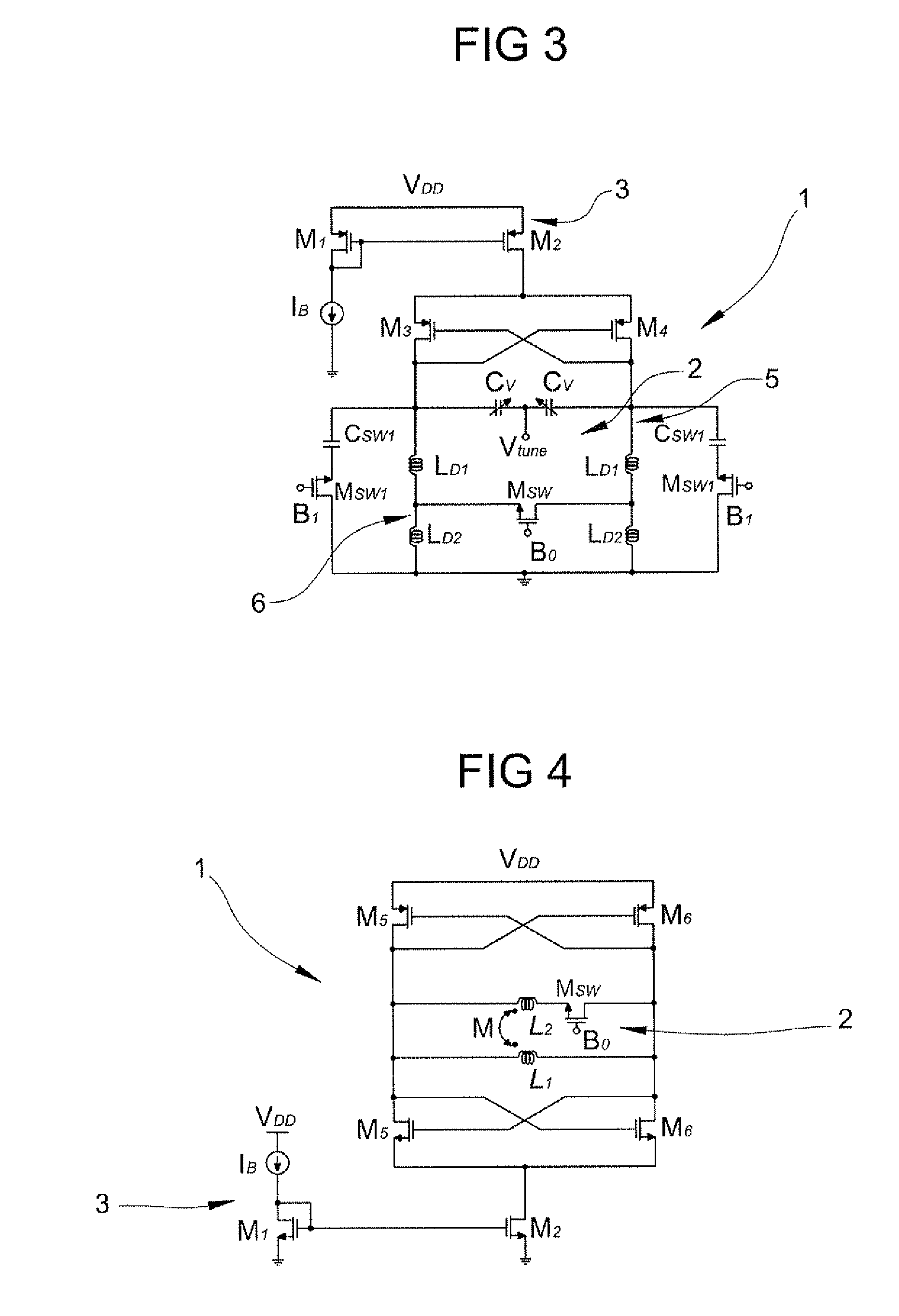
[0035]FIG. 5 illustrates a circuit of a voltage controlled oscillator according to the present invention in which similar elements have been given the same reference numerals as in FIGS. 1-4 previously described. The circuit 1 comprises a bridge structure including two cross-coupled MOS transistors M3 and M4 of the N type and two cross-coupled MOS transistors M5 and M6 of the P type.

[0036]The circuit 1 also comprises an LC resonator 2 placed in parallel between said pairs of transistors M3 and M4 of the N type and M5 and M6 of the P type. The transistors M3, M4, M5 and M6 overall represent the active part of the circuit 1 that has the task of compensating for the losses of the LC resonator 2.

[0037]The two transistors M3 and M4 are connected to a current mirror 3 comprising a pair of transistors Mi and M2 to which a supply voltage VDD is applied. The current mirror 3 generates a current IB used for biasing the circuit 1.

[0038]The same supply voltage VDD is applied to the two transist...


PUM

PropertyMeasurementUnit
Timeaaaaaaaaaa
Electrical inductanceaaaaaaaaaa
Currentaaaaaaaaaa

Abstract

A circuit for a voltage controlled oscillator has a bridge structure including two cross-coupled N-type transistors and two cross-coupled P-type transistors. A current mirror is coupled to the two N-type cross-coupled transistors and configured to generate a bias current. An LC resonator is coupled in parallel between the two cross-coupled N-type transistors and the two P-type cross-coupled transistors. The LC resonator includes two pairs of differential inductors mutually coupled by a mutual inductance coefficient, each pair comprising a first inductor arranged on a respective branch of an external loop, and a second inductor arranged on a respective branch of an internal loop. A first varactor is coupled to a common node and a first branch of the internal loop. A second varactor is coupled to the common node and the second branch of the internal loop.

Description

FIELD OF THE INVENTION[0001]The present invention refers to a circuit for a voltage controlled oscillator (VCO). More specifically, the invention refers to a circuit for a voltage controlled oscillator including a varactor.BACKGROUND OF THE INVENTION[0002]In modern digital wireless telecommunication systems, voltage controlled oscillators (VCO) represent a part for the synthesis of a carrier frequency, thanks to their use in PLL (Phase Locked Loop). In this type of application, the design of the oscillators is made particularly difficult by the high frequency of the synthesised signal, and by the constraints imposed by power consumption.[0003]The traditional topology with LC resonators represents an approach used the most to satisfy the specifications of spectral purity and power consumption imposed by current communication standards. However, there are different aims that push for innovative topologies to be sought, such as the use of CMOS technologies with an ever smaller channel ...

Claims


Application Information

Patent Timeline
IPC IPC(8): H03B5/12H05K13/00
CPCH03B2201/0208H03B2201/0216H03B2201/0266H03B5/1268H03B5/1243Y10T29/49117H03B5/1296H03B5/1215H03B2200/0038H03B5/1265H03B5/124H03B5/1228
Inventor ITALIA, ALESSANDRODIMARTINA, SALVATOREIPPOLITO, CALOGERO MARCOPALMISANO, GIUSEPPE
Owner STMICROELECTRONICS SRL
Why Eureka
Try Eureka