Capacitive load driving circuit

a driving circuit and load technology, applied in the direction of ac-dc network circuit arrangement, ac network voltage adjustment, printing, etc., can solve the problems of difficult to achieve the perfect uniformity, the size of the ink drop to be ejected or the speed thereof, and the operation of the load varies, so as to achieve high-quality images and suppress variations in operation.

Inactive Publication Date: 2011-06-02
SEIKO EPSON CORP
View PDF3 Cites 7 Cited by
  • Summary
  • Abstract
  • Description
  • Claims
  • Application Information

AI Technical Summary

Benefits of technology

[0007]An advantage of some aspects of the invention is to provide a technique that can uniformly operate a plurality of loads by suppressing variations in the operation of the loads while keeping a circuit scale simple by applying one voltage waveform to the plurality of loads.
[0010]The capacitive load can store electric charge therein with the application of voltage, thereby holding the voltage. Therefore, when the connection between the capacitive load and the voltage waveform output unit is released, the capacitive load holds the voltage having been applied thereto as it is upon releasing the connection. By connecting the capacitive load again to the output of the voltage waveform output unit after the voltage of the voltage waveform returns to the voltage range, a voltage waveform output by the voltage waveform output unit can be applied to the capacitive load after that. As a result, it is possible to apply a voltage waveform different from the voltage waveform output by the voltage waveform output unit to each of the capacitive loads. By doing this, even when a voltage waveform output by one voltage waveform output unit is applied to a plurality of capacitive loads, a different voltage waveform can be applied to each of the capacitive loads. Therefore, by previously determining the voltage range of each of the capacitive loads according to the characteristic of each of the capacitive loads, a proper voltage waveform according to the characteristic of each of the capacitive loads can be applied. As a result, even when output of one voltage waveform output unit is applied to a plurality of capacitive loads, variations in operation among the capacitive loads can be suppressed by applying a proper voltage waveform according to the characteristic of each of the capacitive loads and properly operating each of the capacitive loads.
[0013]When the voltage of the voltage waveform increases after releasing the connection of the capacitive load, the voltage of the voltage waveform becomes higher than that held by the capacitive load. Therefore, by connecting the capacitive load with the output of the voltage waveform output unit via the rectifying element disposed in the direction in which current is blocked from flowing into the capacitive load, a change in the voltage of the capacitive load can be blocked until the voltage of the voltage waveform output by the voltage waveform output unit decreases to the voltage of the capacitive load because the current flowing from the voltage waveform output unit to the capacitive load is blocked. When the voltage of the voltage waveform decreases to the voltage of the capacitive load, current starts flowing between the capacitive load and the output of the voltage waveform output unit. Therefore, the capacitive load can be connected to the output of the voltage waveform output unit at a timing in which the voltage of the voltage waveform and the voltage of the capacitive load coincide with each other. Thus, when the voltage of the capacitive load is changed by connecting the capacitive load to the output of the voltage waveform output unit, the voltage of the capacitive load can be smoothly changed. Therefore, a more proper voltage waveform can be applied to the capacitive load.
[0014]Similarly, when the voltage of the voltage waveform decreases after releasing the connection of the capacitive load, by connecting the rectifying element in the direction in which current is blocked from flowing out of the capacitive load, a change in the voltage of the capacitive load can be blocked by blocking current flowing from the capacitive load to the voltage waveform output unit until the decreased voltage of the voltage waveform increases to the voltage of the capacitive load. When the voltage of the voltage waveform increases to the voltage of the capacitive load, the output of the voltage waveform output unit and the capacitive load can be connected at the timing in which the voltage of the voltage waveform and the voltage of the capacitive load coincide with each other. Therefore, a proper voltage waveform whose voltage changes smoothly can be applied to the capacitive load.
[0020]Since using the capacitive load driving circuit according to the above aspect of the invention makes it possible to drive an actuator disposed in an ejection nozzle to properly eject fluid through the ejection nozzle, the invention can be recognized as a fluid ejection device including the load driving circuit, which is still another aspect according to the invention.
[0021]In the fluid ejection device according to this aspect of the invention, variations in operation among actuators can be suppressed due to the load driving circuit. As a result, variations in the amount of fluid or size of fluid drop to be ejected, in the ejecting speed of fluid or the like can be reduced to properly eject fluid.

Problems solved by technology

However, when a voltage waveform generated by one voltage waveform generating circuit is applied to the plurality of loads, there is a problem in that the operation of the loads varies because the characteristics of the individual loads are not perfectly uniform.
In an inkjet printer for example, since it is difficult to achieve the perfect uniformity in the port diameter or channel resistance of an ejection nozzle across a plurality of ejection nozzles, the size of an ink drop to be ejected or the speed thereof varies from ejection nozzle to ejection nozzle even when the same voltage waveform is applied.
Since it is generally difficult to achieve the perfect uniformity in the characteristics of the plurality of loads, such variations in the operation of the loads may generally occur not only in an inkjet printer but also in devices in which a voltage waveform generated by one voltage waveform generating circuit is applied to a plurality of loads.
However, this needs a large number of voltage waveform generating circuits, failing to keep the circuit scale simple.

Method used


Image

  • Capacitive load driving circuit
  • Capacitive load driving circuit
  • Capacitive load driving circuit

Examples


first modified example

C-1. First Modified Example

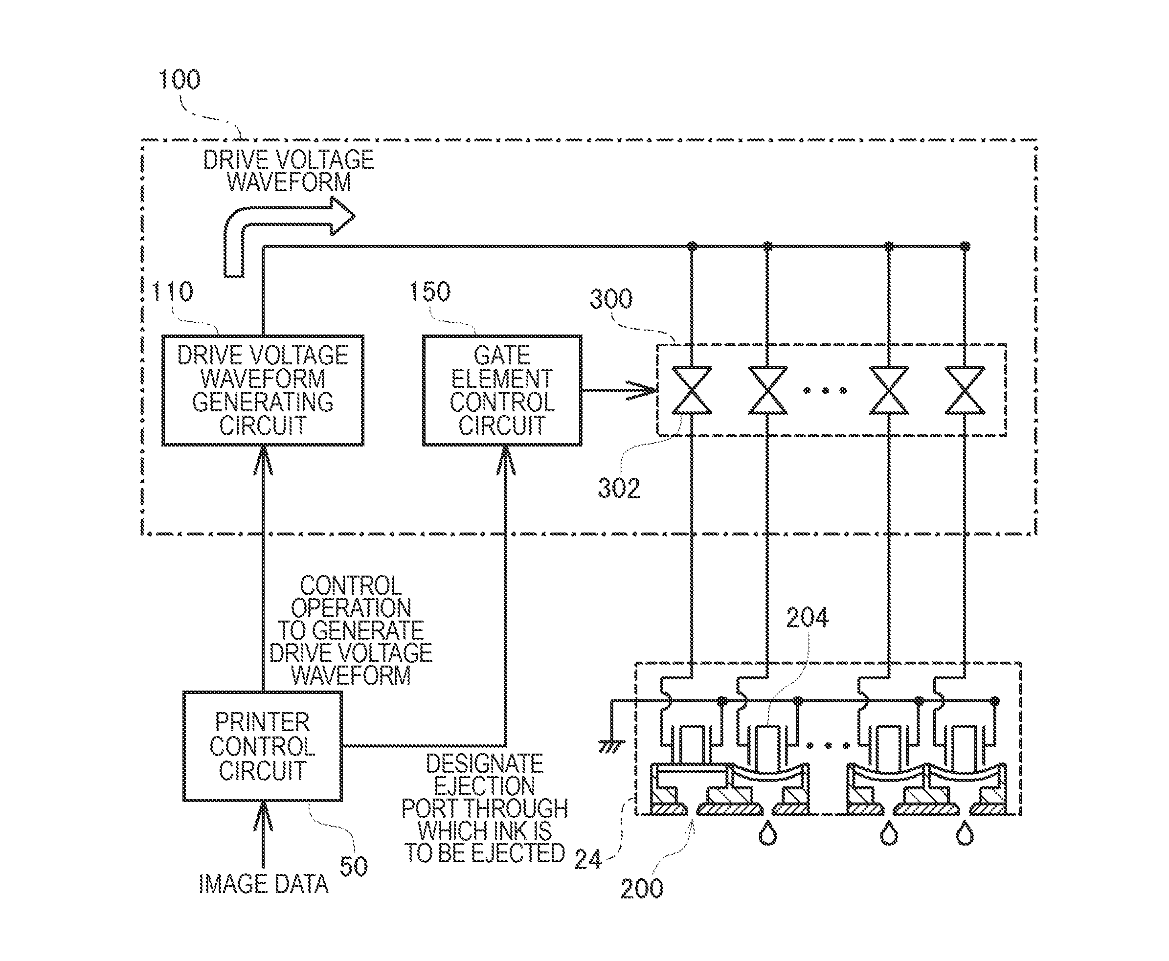
[0071]In applying a drive voltage waveform to the piezo element 204 for driving, current flows from the drive voltage waveform generating circuit 110 toward the piezo element 204 when the voltage of the piezo element 204 increases; and in contrast, current flows from the piezo element 204 toward the drive voltage waveform generating circuit 110 when the voltage of the piezo element 204 decreases. Between the drive voltage waveform generating circuit 110 and the piezo element 204, therefore, a path in which current directed from the drive voltage waveform generating circuit 110 toward the piezo element 204 flows and a path in which current directed from the piezo element 204 toward the drive voltage waveform generating circuit 110 flows are separately disposed, and a gate element is provided in each of the paths, whereby it is possible to select and flow the current flowing in one of the directions. Using such a configuration makes it possible to apply an a...

second modified example

C-2. Second Modified Example

[0081]In the gate unit 300 of the first modified example as described above, even when the gate element is brought into the conductive state earlier than the timing in which the voltage of the drive voltage waveform generating circuit 110 and the voltage of the piezo element 204 coincide with each other, current can be blocked until the voltage of the drive voltage waveform generating circuit 110 and the voltage of the piezo element 204 coincide with each other. In addition, it is possible to allow current to start flowing at an accurate timing in which the voltage of the drive voltage waveform generating circuit 110 and the voltage of the piezo element 204 coincide with each other. Therefore, when the gate element is brought into the conductive state, the gate element may not be brought into the conductive state at the timing in which the voltage of the drive voltage waveform generating circuit 110 and the voltage of the piezo element 204 coincide with e...

third modified example

C-3. Third Modified Example

[0082]In the gate unit 300 of the first modified example, the gate element A and the gate element B are manipulated independently of each other. However, both the gate element A and the gate element B may be manipulated, and further, the so-called exclusive manipulation may be performed in which the gate element B is brought into the disconnection state when the gate element A is brought into the conductive state, while the gate element B is brought into the conductive state when the gate element A is brought into the disconnection state.

[0083]FIGS. 9A to 9C are explanatory diagrams showing a state of applying a voltage waveform to the piezo element using a gate unit of a third modified example where two gate elements are exclusively manipulated. As shown in FIG. 9A, in gate timing data used in the gate unit of the third modified example, it is set to perform the so-called exclusive manipulation in which the gate element B is brought into the “OFF” state w...


PUM


Abstract

A capacitive load driving circuit includes: a voltage waveform output unit that outputs a voltage waveform used for driving a plurality of capacitive loads; and a voltage waveform applying unit that connects each of the plurality of capacitive loads to output of the voltage waveform output unit to thereby apply the voltage waveform to each of the plurality of capacitive loads, wherein the voltage waveform applying unit releases the connection between the capacitive load and the output of the voltage waveform output unit when voltage of the voltage waveform falls outside a voltage range determined for each of the plurality of capacitive loads, and connects the capacitive load to the output of the voltage waveform output unit when the voltage of the voltage waveform falls within the voltage range, to thereby apply a different voltage waveform to each of the plurality of capacitive loads.

Description

BACKGROUND[0001]1. Technical Field[0002]The present invention relates to a technique for applying a voltage to drive a capacitive load.[0003]2. Related Art[0004]A technique for applying a voltage to drive a load of an electronic element such as a semiconductor element or a dielectric element has been widely used in various devices. In a fluid ejection device such as an inkjet printer for example, a voltage is applied to a piezo element that expands and contracts according to the voltage, so that fluid is pushed out of an ejection nozzle and ejected. In a display device such as a liquid crystal display or an organic EL display, a voltage is applied to liquid crystal to align liquid crystal molecules, or a voltage is applied to an organic EL element to cause it to emit light, so that an image is displayed. A technique for applying a voltage to various loads such as a motor or an electromagnet, in addition to the electronic element, to drive the load has also been widely used.[0005]In ...

Claims


Application Information

Patent Timeline
Patent Type & Authority Applications(United States)
IPC IPC(8): B41J29/38H02J4/00
CPCB41J2/04541B41J2/0455B41J2/0459B41J2/04588B41J2/04581
Inventor OSHIMA, ATSUSHITABATA, KUNIOMIYAZAKI, SHINICHIYOSHINO, HIROYUKIIDE, NORITAKA
Owner SEIKO EPSON CORP
Why Eureka
Try Eureka