Electrically contactable grids manufacture
a technology of electrical contact and manufacturing technology, applied in the field of solar cell products, can solve problems such as damage to solar devices
- Summary
- Abstract
- Description
- Claims
- Application Information
AI Technical Summary
Benefits of technology
Problems solved by technology
Method used
Image
Examples
first embodiment
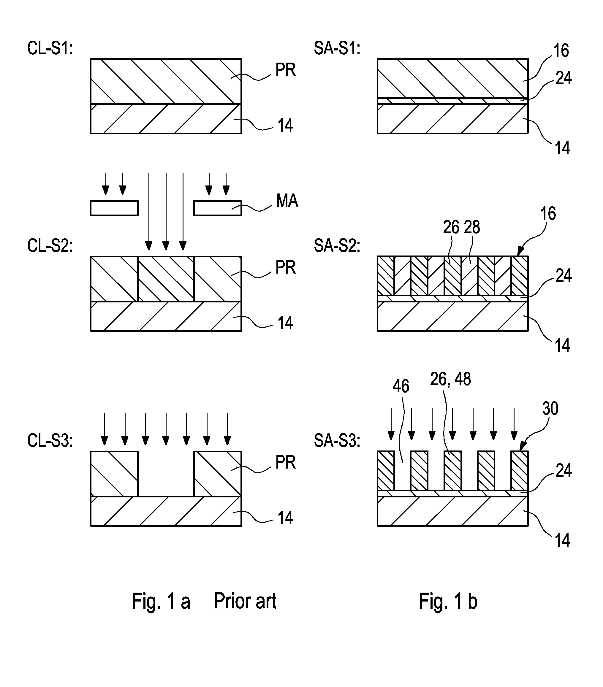
[0044]In contrast thereto, the inventive method illustrated in FIG. 1b includes the step SA-S1 of depositing a heat-sensitive masking agent 16 to the substrate 14. The substrate may be covered with a barrier layer 24 to form an interlayer. The inventive method of the embodiment of FIG. 1b also includes a local heat treatment step SA-S2 of selectively heating of the heat-sensitive masking agent 16 to pattern the masking agent layer 16 into heated parts 26 and non-heated parts 28. The inventive method of FIG. 1B further includes a step SA-S3 of removing the non-heated parts 28 so that openings 46 are formed which give access to the layer 24, and so that heated parts 26 remain as parts 48 masking the substrate 14. In this way, a grid mask 30 is provided that permits a conductive material to be deposited on the substrate 14 (indicated by parallel arrows pointing towards the substrate 14) through the openings 46 of the grid mask 30, usually by a PVD or CVD technique.
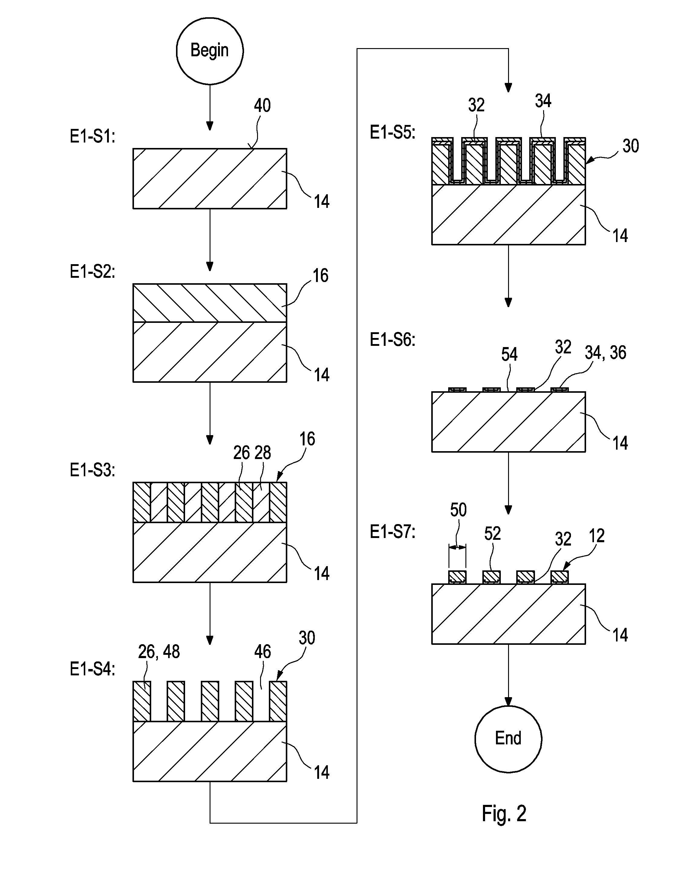
[0045]FIG. 2 shows a ...
second embodiment
[0050]Referring now to FIG. 3, a schematic view of the inventive method is shown. Step E2-S1 also starts from a substrate 14, such as a semiconductor silicon substrate 14 that was prepared with a p-n junction to form a photoactive diode of a solar cell. In step E2-S2 a conductive barrier layer 24, such as titanium (Ti), titanium nitride (TiN), tantalum (Ta) or tantalum nitride (TaN), as a barrier and liner and also as a conductive intermediate layer 24, is deposited onto the substrate surface 40. In step E2-S3, a masking agent layer 16, such as a copolymer including PMMA (polymethylmethacrylate) and PS (polystyrene), is deposited onto the layer 24. The layer 24 includes electrically conductive material that is arranged on the substrate 14.
[0051]Local heating in step E2-S4, such as by using a patterned heat stamp, forms heated parts 26 and non-heated parts 28 in the masking agent layer 16. The copolymer separates into heated areas (heated parts 26) containing mainly PS, and non-heate...
third embodiment
[0054]FIG. 4 depicts sub-steps of the inventive method for forming a grid mask 30. Starting from an initial step E3-S1, a substrate 14, such as a semiconductor silicon substrate 14 that was prepared with a p-n junction to form a photoactive diode of a solar cell, is coated with an antireflective layer 22. During the next step E3-S2 the antireflective layer 22 is coated by a masking agent layer 16. This masking agent layer 16 can include a copolymer (as described in the embodiment above) or a thermoresist material, the latter which can be deposited by spin coating, spray coating and the like.
[0055]The structuring in step E3-S3 is performed by a so-called heat stamping technique using a kind of heated “brand iron” as heat stamp 38. By pressing the patterned heat stamp 38 on the masking agent layer 16, heated areas 26 and non-heated areas 28 of the masking agent layer 16 are formed, as is shown in step E3-S4. The following step E3-S5 includes an etching procedure for removing selected ...
PUM
 Abstract
Description
Claims
Application Information
 - R&D
- Intellectual Property
- Life Sciences
- Materials
- Tech Scout
- Unparalleled Data Quality
- Higher Quality Content
- 60% Fewer Hallucinations
Browse by: Latest US Patents, China's latest patents, Technical Efficacy Thesaurus, Application Domain, Technology Topic, Popular Technical Reports.
© 2025 PatSnap. All rights reserved.Legal|Privacy policy|Modern Slavery Act Transparency Statement|Sitemap|About US| Contact US: help@patsnap.com


