
Substrate processing apparatus

a processing apparatus and substrate technology, applied in the field of substrate processing apparatus, can solve the problems of significant impact of processing cost on unit price, device price, and manufacturing cost of electronic devices,

Active Publication Date: 2011-02-17
BOOKS AUTOMATION US LLC
View PDF99 Cites 66 Cited by
  • Summary
  • Abstract
  • Description
  • Claims
  • Application Information

AI Technical Summary

Benefits of technology

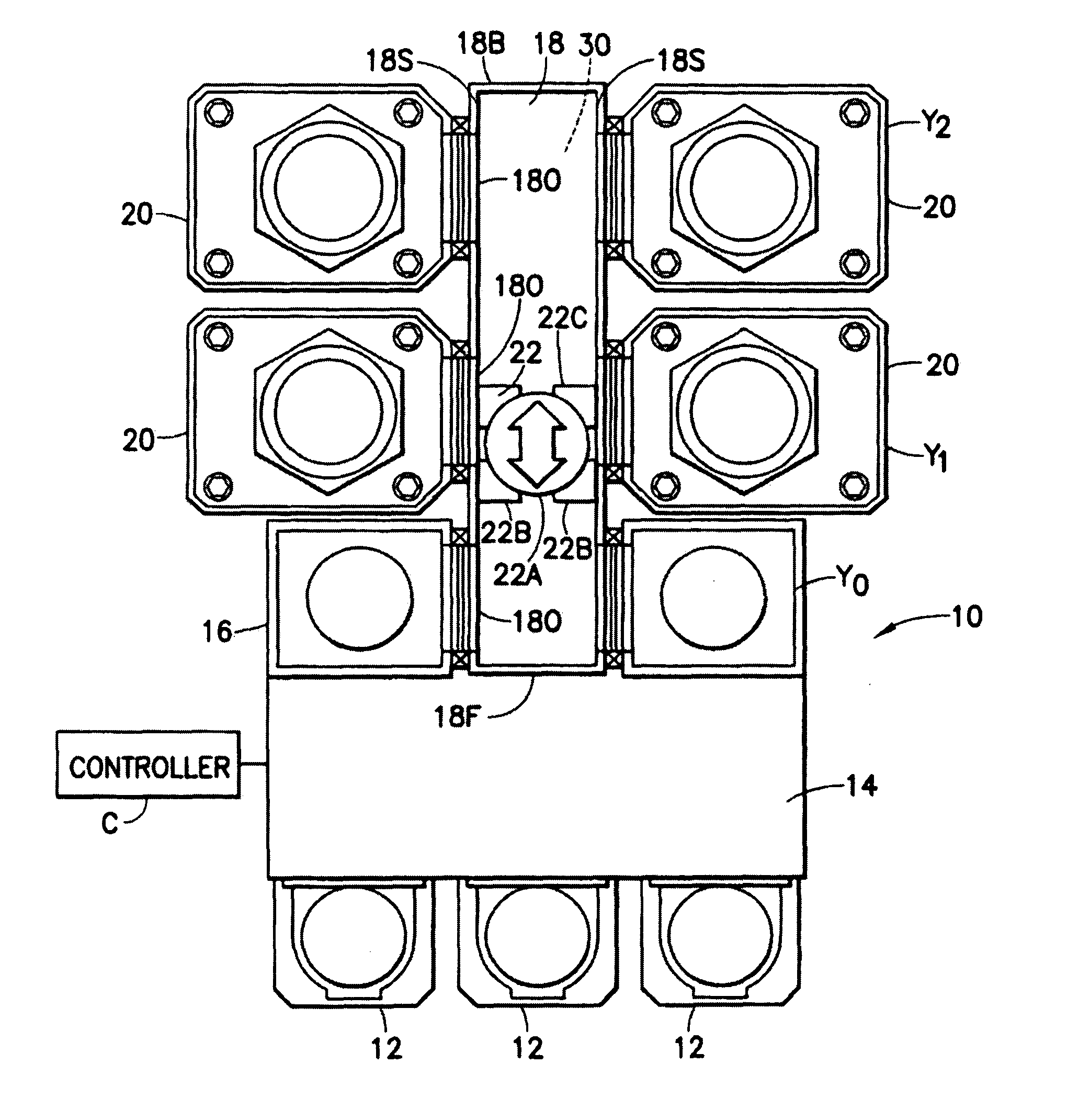
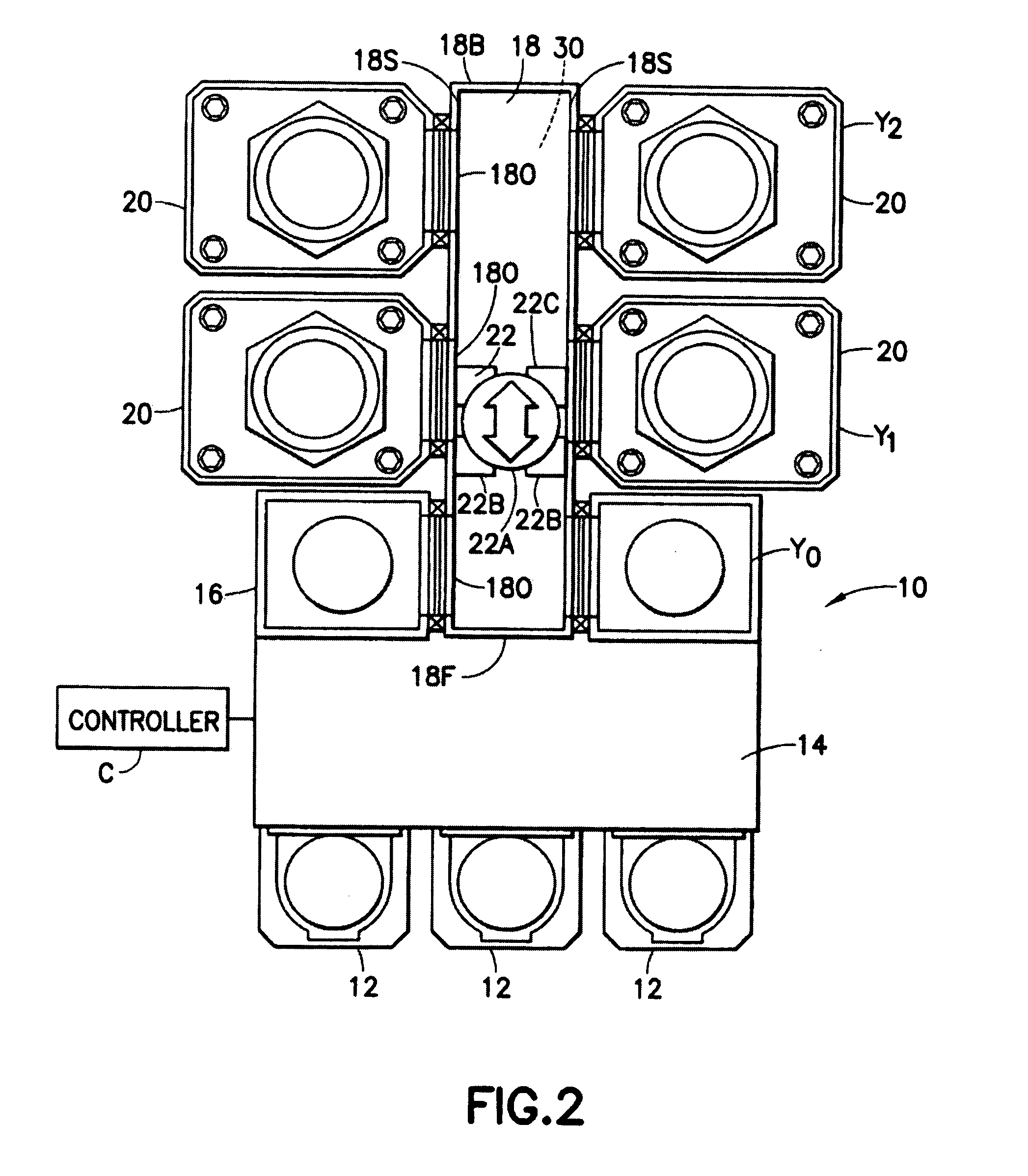
[0006]In accordance with the first embodiment, a substrate processing apparatus is provided. The apparatus comprises a transport chamber, at least one substrate holding module for holding a substrate, a transport vehicle, and another module. The transport chamber is capable of having a controlled atmosphere therein. The at least one substrate holding module is communicably connected to the transport chamber for allowing transfer of the substrate between the at least one holding module and the transport chamber. The transport vehicle is movably mounted in the transport chamber. The vehicle has a base and a substrate transfer arm that is movably jointed and movably mounted to the base. The other module is capable of holding the substrate and is communicably connected to the transport chamber for transferring the chamber to the substrate therebetween. The transport chamber defines a linear travel slot for the vehicle. The at least one holding module is located on one side of the slot, and the arm has articulation for moving a substrate to opposite sides of the slot. This allows the other module to be selectively connected to the transport chamber on either side of the slot. The transport vehicle can effect transfer of the substrate between the transport chamber and both the holding module and the other module.

Problems solved by technology

One of the factors affecting consumer desire for new electronic devices naturally is the price of the device.
A significant portion of the manufacturing costs for electronic devices is the cost of producing the electronics which starts with the manufacturing and processing of semi-conductor substrates such as used in manufacturing electronic components, or panels used for making displays.
The cost of processing significant impact on unit price).
However, it appears that conventional processing apparatus have reached a dead end with respect to size reduction.
Moreover, conventional processing apparatus appear to have reached a limit with respect to increasing throughput per unit.
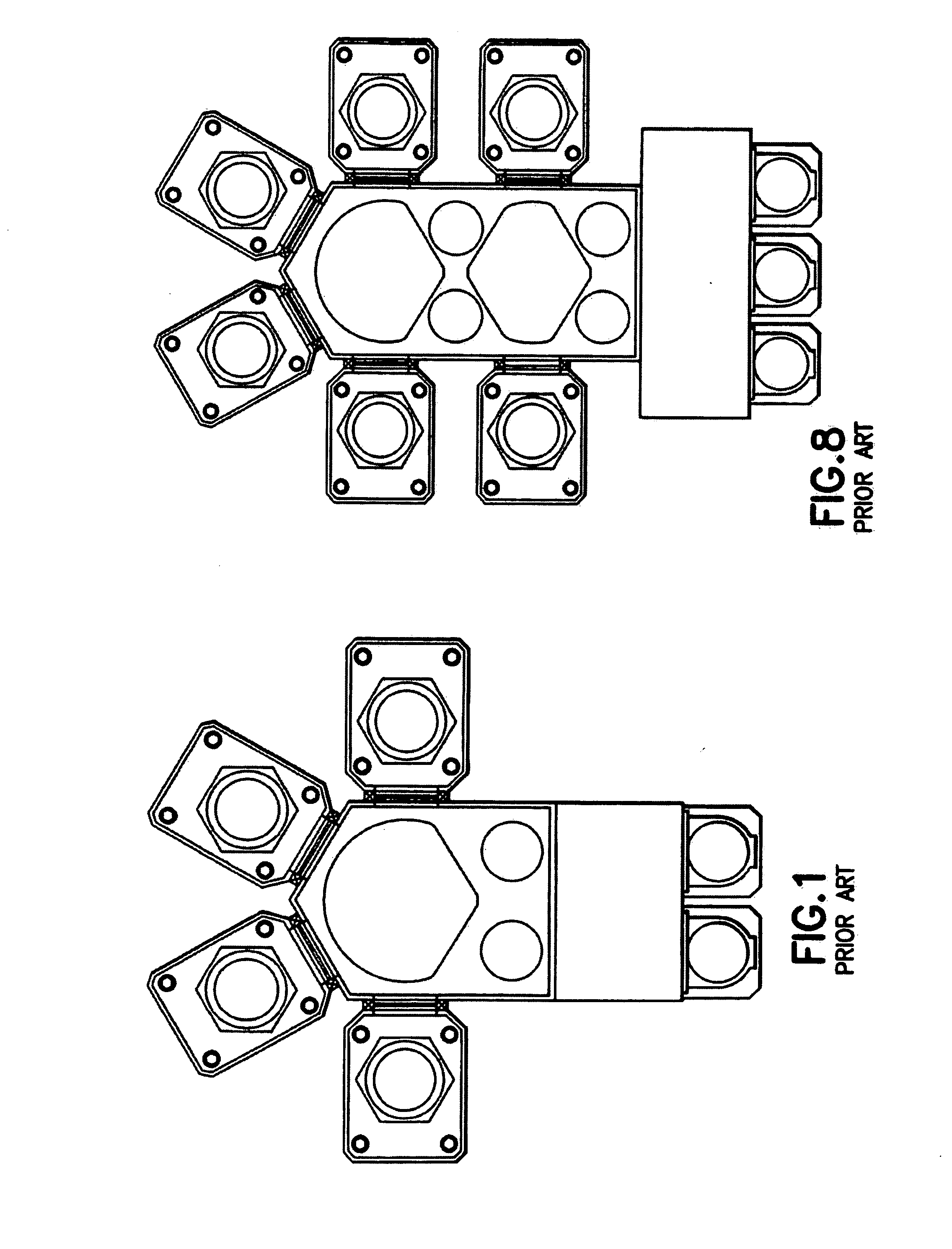
As can be realized from FIG. 1, throughput of the conventional processing apparatus is limited by the handling rate of the transport apparatus.

Method used


Image

  • Substrate processing apparatus
  • Substrate processing apparatus
  • Substrate processing apparatus

Examples


Embodiment Construction

[0006]In accordance with the first embodiment, a substrate processing apparatus is provided. The apparatus comprises a transport chamber, at least one substrate holding module for holding a substrate, a transport vehicle, and another module. The transport chamber is capable of having a controlled atmosphere therein. The at least one substrate holding module is communicably connected to the transport chamber for allowing transfer of the substrate between the at least one holding module and the transport chamber. The transport vehicle is movably mounted in the transport chamber. The vehicle has a base and a substrate transfer arm that is movably jointed and movably mounted to the base. The other module is capable of holding the substrate and is communicably connected to the transport chamber for transferring the chamber to the substrate therebetween. The transport chamber defines a linear travel slot for the vehicle. The at least one holding module is located on one side of the slot, ...


PUM

PropertyMeasurementUnit
Angleaaaaaaaaaa
Transport propertiesaaaaaaaaaa

Abstract

A semiconductor workpiece processing apparatus having a first chamber, a transport vehicle, and another chamber. The first chamber is capable of being isolated from an outside atmosphere. The transport vehicle is located in the first chamber and is movably supported from the first chamber for moving linearly relative to the first chamber. The transport vehicle includes a base, and an integral semiconductor workpiece transfer arm movably mounted to the base and capable of multi-access movement relative to the base. The other chamber is communicably connected to the first chamber via a closable opening of the first chamber. The opening is sized to allow the transport vehicle to transit between the first chamber and the other chamber through the opening.

Description

CROSS-REFERENCE TO RELATED APPLICATION(S)[0001]This application claims the benefit of U.S. patent application Ser. No. 10 / 624,987, filed 22 Jul. 2003, which claims the benefit of Provisional Application No. 60 / 397,895, filed Jul. 22, 2002, all of which are incorporated by reference herein in their entireties.BACKGROUND INFORMATION[0002]1. Field[0003]The embodiments and methods described herein relate to substrate processing apparatus and, more particularly, to substrate processing apparatus with chambers interconnected in a Cartesian arrangement.[0004]2. Brief Description of Earlier Developments[0005]One of the factors affecting consumer desire for new electronic devices naturally is the price of the device. Conversely, if the cost, and hence the price of new electronic devices can be lowered, it would appear that a beneficial effect would be achieved in consumer desires for new electronic devices. A significant portion of the manufacturing costs for electronic devices is the cost o...

Claims


Application Information

Patent Timeline
IPC IPC(8): H01L21/673H01L21/677H01L21/67
CPCH01L21/67742H01L21/67196
Inventor HOFMEISTER, CHRISTOPHERCAVENEY, ROBERT T.
Owner BOOKS AUTOMATION US LLC
Learn More