
Design Optimization for Circuit Migration

a technology of design optimization and circuit migration, applied in the direction of cad circuit design, program control, instruments, etc., can solve the problems of process variations between, problems that are typically discovered, and process drawbacks, and achieve the effect of minimizing the violation of timing performance parameters

Active Publication Date: 2011-02-10
TAIWAN SEMICON MFG CO LTD
View PDF37 Cites 7 Cited by
  • Summary
  • Abstract
  • Description
  • Claims
  • Application Information

AI Technical Summary

Benefits of technology

[0006]These and other problems are generally solved or circumvented, and technical advantages are generally achieved, by embodiments of the present invention which minimize the man hours and effort expended on the design of the shrink node technology while maintaining comparable design quality.
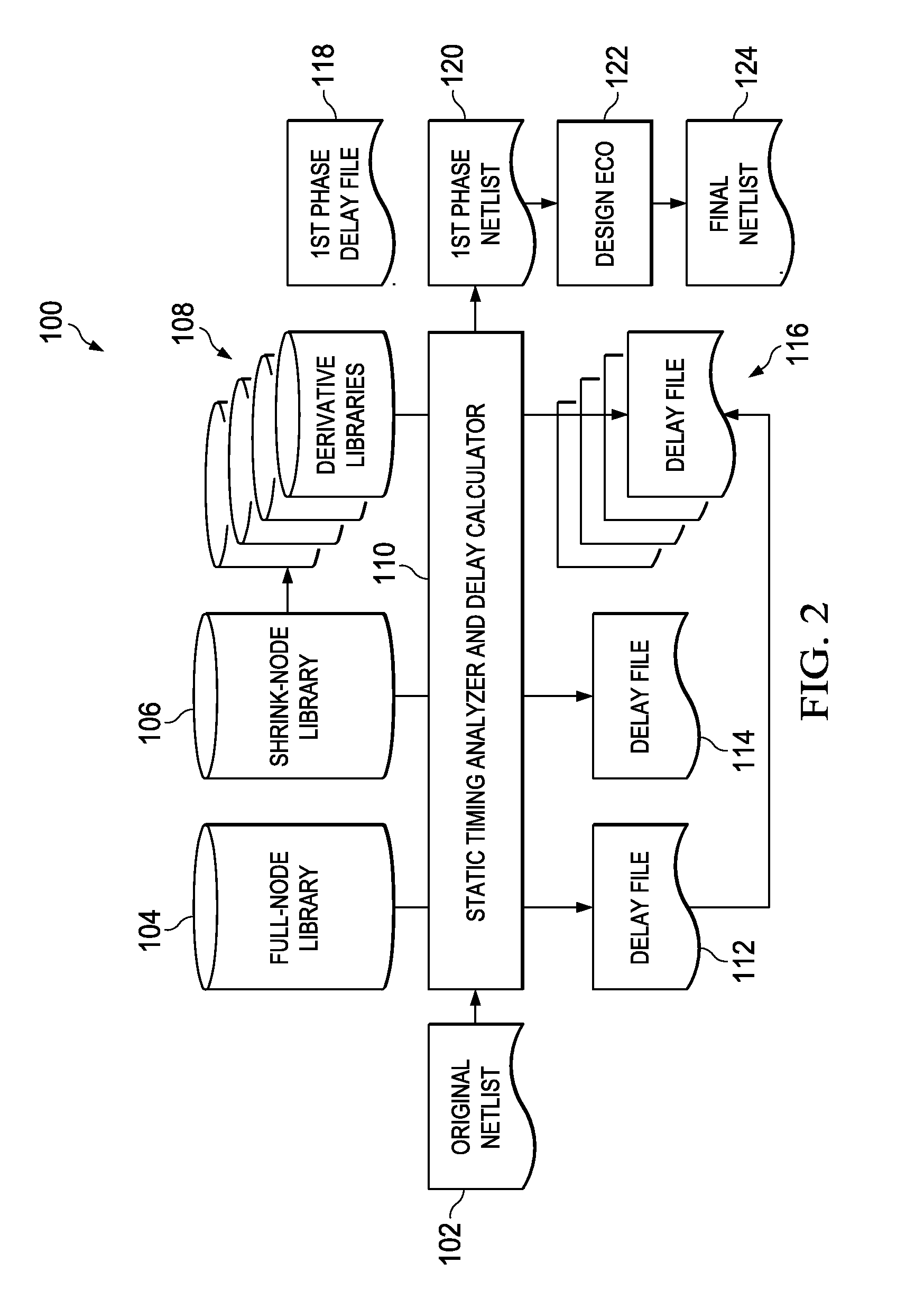
[0009]In accordance with another embodiment of the present invention, a method for providing an adjusted electronic representation of an integrated circuit layout comprises generating full node cells from a full node netlist, scaling the full node cells to provide shrink node cells, providing a timing performance of the full node cells and the shrink node cells, comparing the timing performance of the full node cells to the timing performance of the shrink node cells, generating derivative cells of at least one shrink node cell, providing a timing performance of the derivative cells, comparing the timing performance of the derivative cells to the timing performance of the full node cells, and providing a first netlist comprising at least one derivative cell that minimizes a difference between the timing performance of the at least one shrink node cell and a corresponding full node cell. Each derivative cell comprises a variation of the at least one shrink node cell.
[0010]In accordance with a further embodiment of the present invention, a method for providing an adjusted electronic representation of an integrated circuit layout comprises providing a timing performance of a path in a first netlist, identifying a first cell in the path that violates a timing performance parameter, providing a first modified netlist comprising a variation of the first netlist to compensate for the first cell in the path that violates the timing performance parameter, and providing a final netlist. The variation includes a first derivative cell of the first cell or a subsequent derivative cell of a subsequent cell that is in the path after the first cell such that the violation of the timing performance parameter is minimized.

Problems solved by technology

However, these processes are not without their drawbacks.
Scaling down a layout in this manner usually results in process variations between the technology nodes and in performance variation.
Some process variations that may arise are problems in gate processing, such as forming gate spacers, gate oxide thickness, metal thickness, etching bias, mask making, and optical proximity correction (OPC).
The problems typically would be discovered during implementation, such as by using electronic design automation (EDA) software.
These processes thus generally use many man-hours to bring the scaled down layout to tape-out.

Method used


Image

  • Design Optimization for Circuit Migration
  • Design Optimization for Circuit Migration
  • Design Optimization for Circuit Migration

Examples


Embodiment Construction

[0016]The making and using of the present embodiments are discussed in detail below. It should be appreciated, however, that the present invention provides many applicable inventive concepts that can be embodied in a wide variety of specific contexts. The specific embodiments discussed are merely illustrative of specific ways to make and use the invention, and do not limit the scope of the invention.

[0017]The present invention will be described with respect to embodiments in a specific context, namely the migration of an integrated circuit chip layout to a smaller technology node, such as in shrink technology. The invention may also be applied, however, to the migration of an integrated circuit chip layout to a larger technology node.

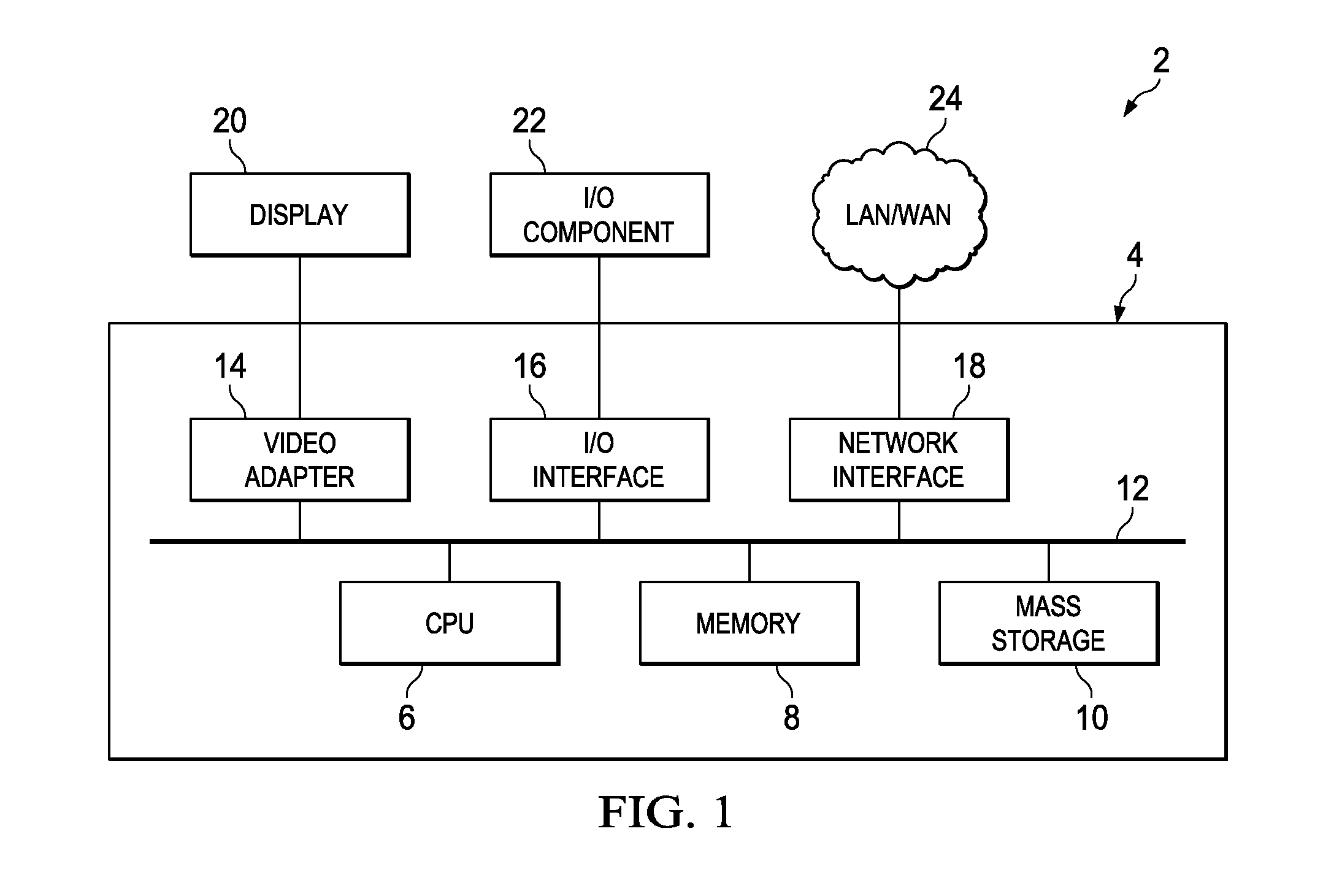
[0018]Referring now to FIG. 1, a block diagram of a processing system 2 is provided in accordance with an embodiment of the present invention. The processing system 2 is a general purpose computer platform and may be used to implement any or all of the ...


PUM


Abstract

An embodiment of the present invention is a computer program product for providing an adjusted electronic representation of an integrated circuit layout. The computer program product has a medium with a computer program embodied thereon. Further, the computer program comprises computer program code for providing full node cells from a full node netlist, computer program code for scaling the full node cells to provide shrink node cells, computer program code for providing a timing performance of the full node cells and the shrink node cells, computer program code for comparing the timing performance of the full node cells to the timing performance of the shrink node cells, and computer program code for providing a first netlist.

Description

[0001]This application claims the benefit of U.S. Provisional patent application Ser. No. 61 / 231,520, filed on Aug. 5, 2009, and entitled “Design Optimization for Circuit Migration,” which application is incorporated herein by reference.TECHNICAL FIELD[0002]The present invention relates generally to a method and computer program product for semiconductor device design, and more particularly to a method and computer program product for the design of a semiconductor device migrating to a smaller technology node.BACKGROUND[0003]Generally in integrated circuit design, integrated circuit chip layouts are commonly shrunk, or scaled, to smaller technology nodes to reduce product costs and extend the product's life cycle. Processes that realized this shrinking or scaling are generally known as shrink technology. However, these processes are not without their drawbacks.[0004]Known processes typically require a designer to scale down by a fixed factor a taped-out chip layout from one technolo...

Claims


Application Information

Patent Timeline
IPC IPC(8): G06F17/50
CPCG06F17/5068G06F17/5081G06F17/505G06F30/39G06F30/398G06F30/327G06F30/392G06F30/396
Inventor LU, LEE-CHUNGCHENG, YI-KANWANG, CHUNG-HSINGHUANG, CHEN-FU ALEXCHAO, HSIAO-SHUCHIANG, CHIN-YUYU, HO CHETSAI, CHIH SHENGYING, SHU YI
Owner TAIWAN SEMICON MFG CO LTD
Learn More