
Organic light emitting display apparatus and method of manufacturing organic light emitting display apparatus

a technology of which is applied in the direction of electric lighting source, solid-state device, light source, etc., can solve the problems of ir drop, poor performance of thin top emission organic light emitting display apparatus

Active Publication Date: 2011-02-10
SAMSUNG DISPLAY CO LTD
View PDF8 Cites 23 Cited by
  • Summary
  • Abstract
  • Description
  • Claims
  • Application Information

AI Technical Summary

Benefits of technology

[0010]Aspects of embodiments of the present invention are directed toward an organic light emitting display apparatus capable of preventing or protecting from both an IR drop and a decrease in a contrast ratio, and a method of manufacturing an organic light emitting display apparatus.
[0011]Aspects of embodiments of the present invention are directed toward an organic light emitting display apparatus having a high contrast ratio capable of preventing or protecting from an IR drop and a method of manufacturing an organic light emitting display apparatus.

Problems solved by technology

Moreover, since a plurality of thin film transistors are used to control pixels, performance of an organic light emitting display apparatus may be poor.
However, since a top electrode, that is, an opposite electrode, of a top emission-type organic light emitting display apparatus needs to be a transparent electrode, the top emission-type organic light emitting display apparatus is thin and may have high resistance, causing an IR drop.

Method used


Image

  • Organic light emitting display apparatus and method of manufacturing organic light emitting display apparatus
  • Organic light emitting display apparatus and method of manufacturing organic light emitting display apparatus
  • Organic light emitting display apparatus and method of manufacturing organic light emitting display apparatus

Examples


Embodiment Construction

[0037]In the following detailed description, only certain exemplary embodiments of the present invention are shown and described, by way of illustration. As those skilled in the art would recognize, the invention may be embodied in many different forms and should not be construed as being limited to the embodiments set forth herein. Also, in the context of the present application, when an element is referred to as being “on” another element, it can be directly on the another element or be indirectly on the another element with one or more intervening elements interposed therebetween. Like reference numerals designate like elements throughout the specification.

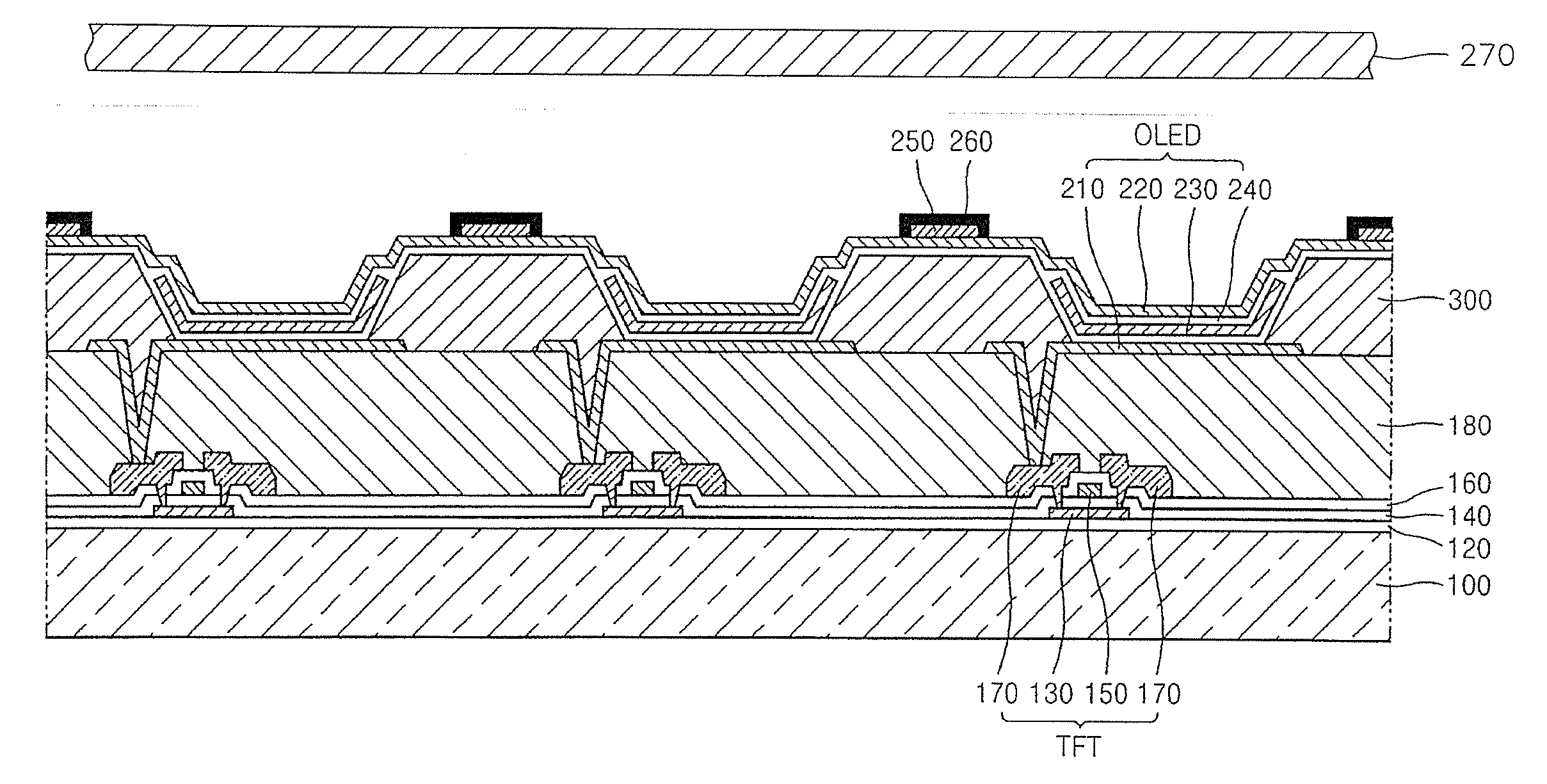
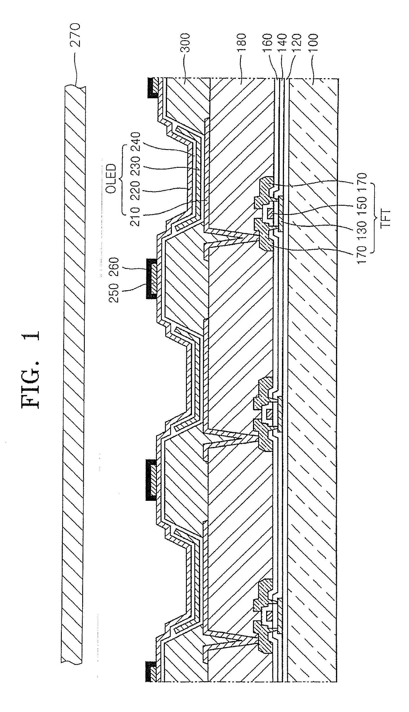
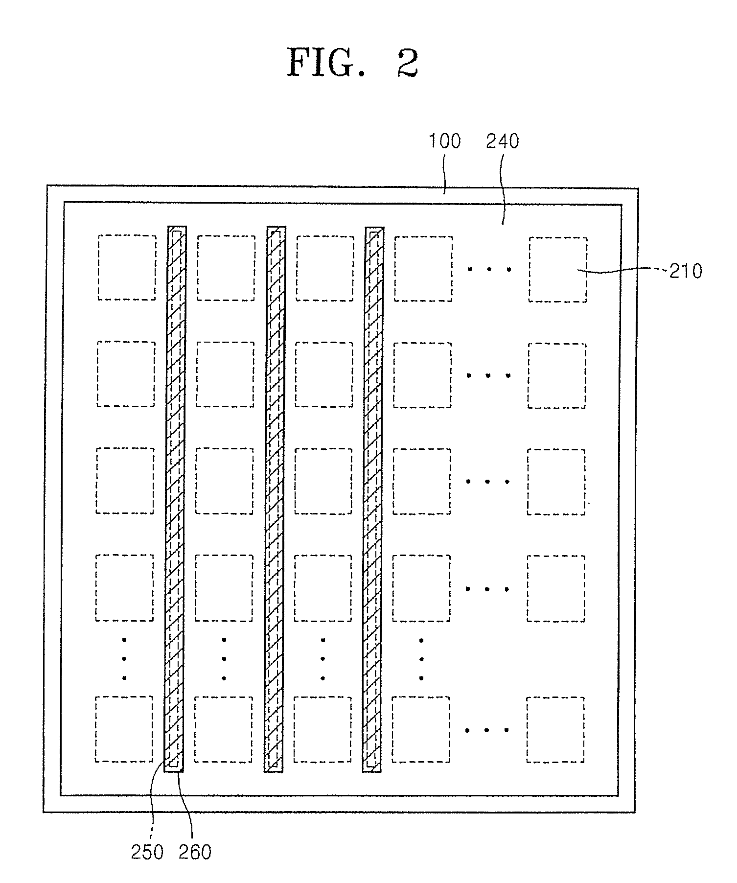
[0038]FIG. 1 is a schematic sectional view of an organic light emitting display apparatus according to an embodiment of the present invention, and FIG. 2 is a schematic plan view of the organic light emitting display apparatus of FIG. 1.

[0039]Referring to FIG. 1, a plurality of thin film transistors (TFTs) are disposed on a sub...


PUM


Abstract

An organic light emitting display apparatus capable of preventing or reducing an IR drop and a decrease in a contrast ratio, and a method of manufacturing the same. The organic light emitting display apparatus includes: a substrate; a plurality of thin film transistors on the substrate; a plurality of organic light emitting diodes, each of the organic light emitting diodes including: a pixel electrode electrically connected to a corresponding one of the thin film transistors, a portion of an opposite electrode, the opposite electrode being above the substrate and covering all of the substrate, and an intermediate layer between the pixel electrode and the opposite electrode and comprising at least an organic light emitting layer; an opposite electrode bus line between adjacent pixel electrodes of the organic light emitting diodes on the opposite electrode of the organic light emitting diodes; and a black matrix surrounding the opposite electrode bus line.

Description

CROSS-REFERENCE TO RELATED PATENT APPLICATION[0001]This application claims priority to and the benefit of Korean Patent Application No. 10-2009-0073519, filed on Aug. 10, 2009, in the Korean Intellectual Property Office, the entire content of which is incorporated herein by reference.BACKGROUND[0002]1. Field[0003]The present invention relates to an organic light emitting display apparatus and a method of manufacturing an organic light emitting display apparatus.[0004]2. Description of the Related Art[0005]An organic light emitting display apparatus produces light in accordance with the following principle: when an electrical signal is applied to a cathode and an anode, holes injected from the anode move to a light emitting layer and electrons injected from the cathode move to the light emitting layer. Then, in the light emitting layer, holes and electrons are combined to form excitons, and the excitons change from an excited state to a ground state, thereby producing light.[0006]Org...

Claims


Application Information

Patent Timeline
IPC IPC(8): H01L51/52H01L51/56H05B44/00
CPCH01L27/3279H01L51/5284H01L51/5228H01L51/5212H10K59/1315H10K59/80516H10K59/8792H10K59/80522H10K59/131H10K50/814H10K50/824H10K50/865
Inventor SUH, MIN-CHUL
Owner SAMSUNG DISPLAY CO LTD
Learn More