Method for obtaining high performance thin film devices deposited on highly textured substrates
a technology of thin film and substrate, applied in the field of thin film solar cells, can solve the problem of significant price drop per watt peak capacity
- Summary
- Abstract
- Description
- Claims
- Application Information
AI Technical Summary
Benefits of technology
Problems solved by technology
Method used
Image
Examples
Embodiment Construction
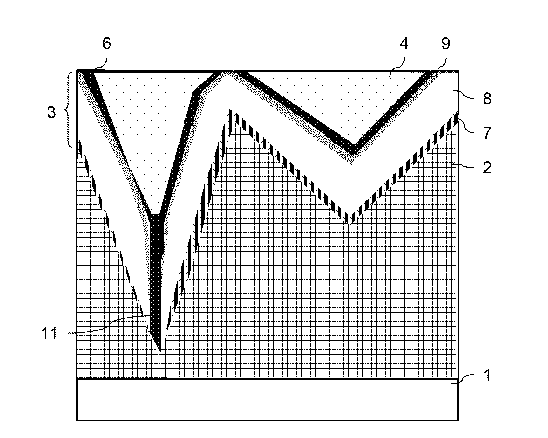
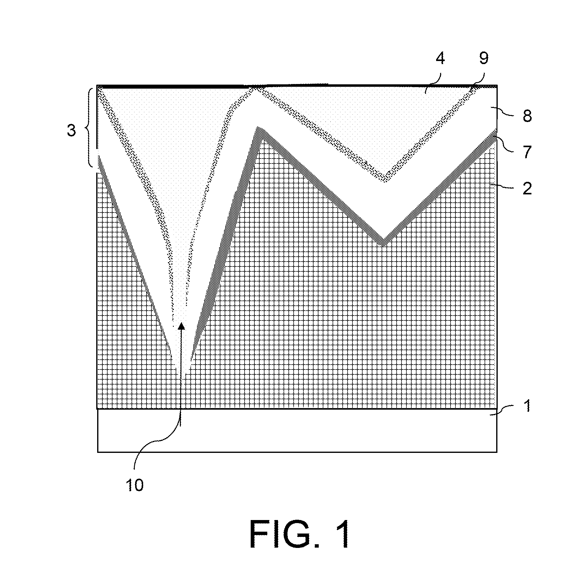
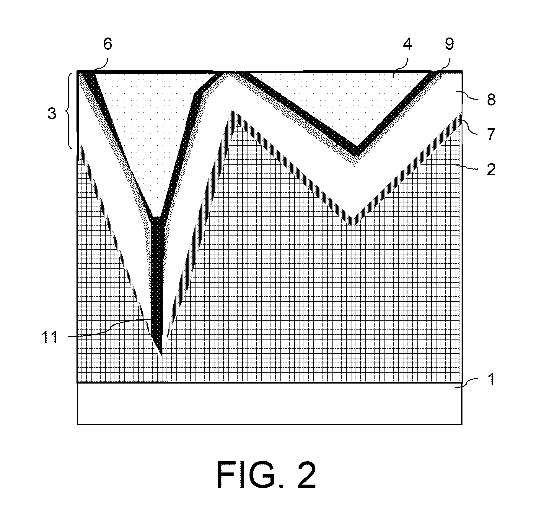
[0061]FIG. 1 shows a cross-section through a conventional basic thin film solar cell with pin-structured absorber layer. A textured conductive TCO layer 2 is deposited on a substrate 1. On top of this TCO layer an absorber layer 3 is deposited that consists of a p-layer 7, i.e. a layer of a positively doped semiconductor, followed by an i-layer 8, i.e. a layer of an intrinsic semiconductor, followed by an n-layer 9, i.e. a layer of a negatively doped semiconductor. A second conductive TCO layer 4 is deposited on top of the absorber layer. Light is entering the solar cell through the substrate 1, enters the textured TCO layer 2 and is scattered into the absorber layer 3 where the conversion of light into electric energy takes place. The TCO layers (2, 4) serve as electrical contacts of the solar cell. As the absorber layer is not well deposited in the valleys of the textured TCO layer the TCO layers 2 and 4 form a direct electrical contact which leads to a low resistance path 10 and ...
PUM
 Abstract
Description
Claims
Application Information
 - R&D
- Intellectual Property
- Life Sciences
- Materials
- Tech Scout
- Unparalleled Data Quality
- Higher Quality Content
- 60% Fewer Hallucinations
Browse by: Latest US Patents, China's latest patents, Technical Efficacy Thesaurus, Application Domain, Technology Topic, Popular Technical Reports.
© 2025 PatSnap. All rights reserved.Legal|Privacy policy|Modern Slavery Act Transparency Statement|Sitemap|About US| Contact US: help@patsnap.com


