Method and system for communicating via leaky wave antennas on high resistivity substrates

a leaky wave antenna and substrate technology, applied in the field of wireless communication, can solve the problems of power inefficiency of transmitters and/or receivers in comparison to other blocks of portable communication devices

Inactive Publication Date: 2010-12-09
AVAGO TECH WIRELESS IP SINGAPORE PTE
View PDF102 Cites 43 Cited by
  • Summary
  • Abstract
  • Description
  • Claims
  • Application Information

AI Technical Summary

Benefits of technology

[0019]FIG. 8 is a diagram illustrating wireless communication via leaky wave antennas integrated in a high resistivity substrate, in accordance with an embodiment of the invention.
[0020...

Problems solved by technology

Additionally, transmit and/or receive circuitry within such mobile wireless devices often account for a significant portion of the power consumed within these devices.
Mor...

Method used


Image

  • Method and system for communicating via leaky wave antennas on high resistivity substrates
  • Method and system for communicating via leaky wave antennas on high resistivity substrates
  • Method and system for communicating via leaky wave antennas on high resistivity substrates

Examples


Embodiment Construction

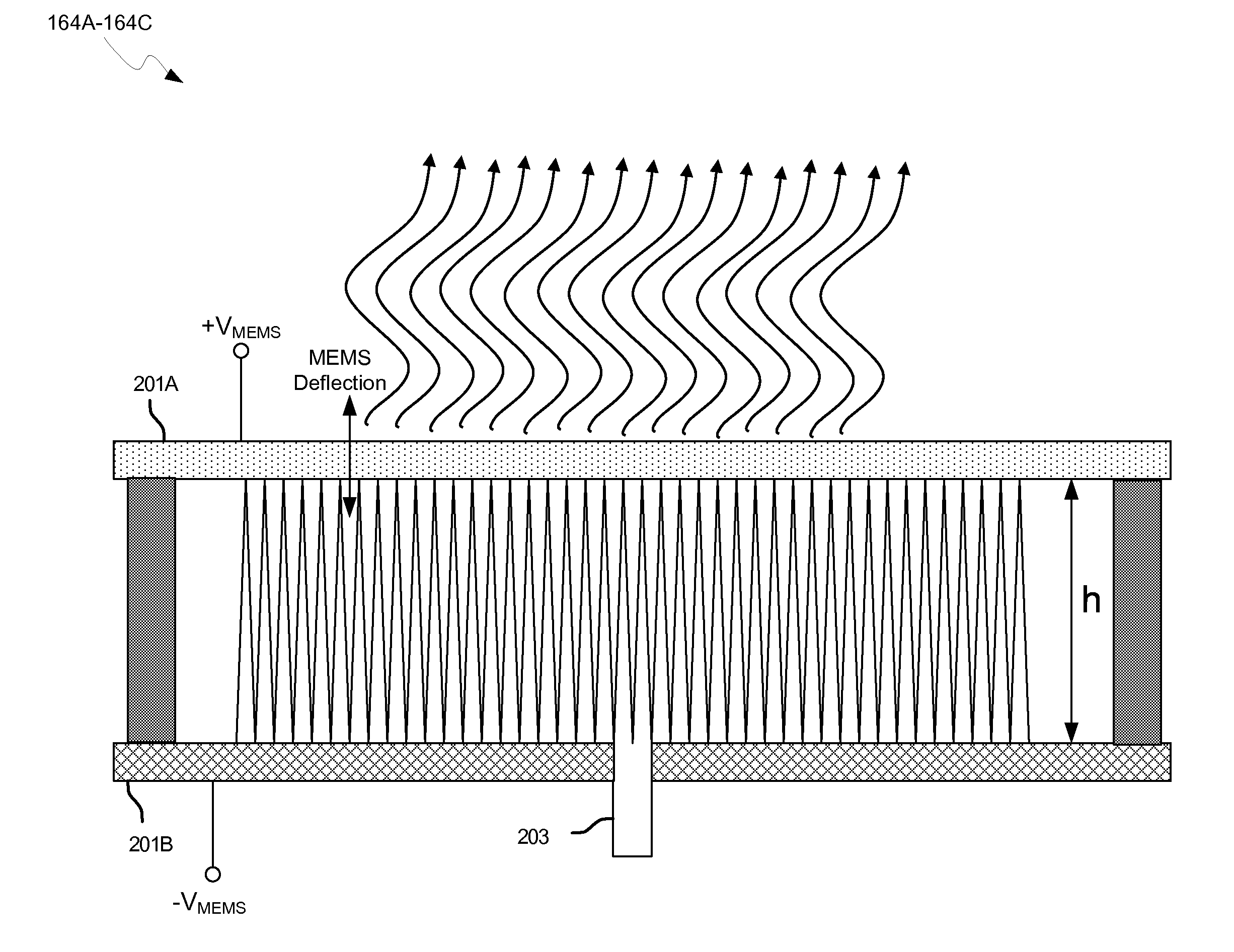
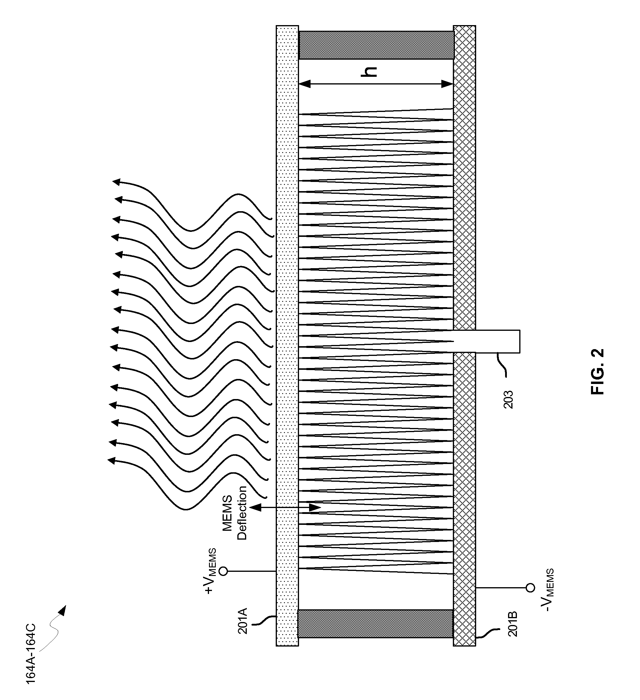
[0021]Certain aspects of the invention may be found in a method and system for communicating via leaky wave antennas on high resistivity substrates. Exemplary aspects of the invention may comprise communicating RF signals using one or more leaky wave antennas that may be integrated within an integrated circuit comprising a high resistivity substrate. The high resistivity substrate may comprise a silicon-on-sapphire substrate. The leaky wave antennas integrated within the integrated circuit may be configured to transmit the RF signals at a desired angle from the surface of the integrated circuit. The RF signals may be communicated between regions within the integrated circuit. The leaky wave antennas comprise microstrip waveguides where the cavity height of the one or more of the leaky wave antennas may be configured by controlling spacing between conductive lines in the microstrip waveguides. The leaky wave antennas may comprise coplanar waveguides where a cavity height of the one o...


PUM


Abstract

Methods and systems for communicating via leaky wave antennas (LWAs) on high resistivity substrates are disclosed and may include communicating RF signals using one or more LWAs that may be integrated in an integrated circuit (chip) comprising a high resistivity substrate, which may include a silicon-on-sapphire substrate. The LWAs integrated in the chip may be configured to transmit the RF signals at a desired angle from the surface of the chip. The RF signals may be communicated between regions within the chip. The LWAs may include microstrip or coplanar waveguides where the cavity height of the one or more of the LWAs may be configured by controlling spacing between conductive lines in the waveguides. The RF signals may be communicated from the LWAs integrated in the chip to LWAs in a package to which the chip is bonded or in a printed circuit board to which the package is bonded.

Description

CROSS-REFERENCE TO RELATED APPLICATIONS / INCORPORATION BY REFERENCE[0001]This application makes reference to, claims the benefit from, and claims priority to U.S. Provisional Application Ser. No. 61 / 246,618 filed on Sep. 29, 2009, and U.S. Provisional Application Ser. No. 61 / 185,245 filed on Jun. 9, 2009.[0002]This application also makes reference to:U.S. patent application Ser. No. 12 / 650,212 filed on Dec. 30, 2009;U.S. patent application Ser. No. 12 / 650,295 filed on Dec. 30, 2009;U.S. patent application Ser. No. 12 / 650,277 filed on Dec. 30, 2009;U.S. patent application Ser. No. 12 / 650,192 filed on Dec. 30, 2009;U.S. patent application Ser. No. 12 / 650,224 filed on Dec. 30, 2009;U.S. patent application Ser. No. 12 / 650,176 filed on Dec. 30, 2009;U.S. patent application Ser. No. 12 / 650,246 filed on Dec. 30, 2009;U.S. patent application Ser. No. 12 / 650,292 filed on Dec. 30, 2009;U.S. patent application Ser. No. 12 / 650,324 filed on Dec. 30, 2009;U.S. patent application Ser. No. 12 / 708,36...

Claims


Application Information

Patent Timeline
IPC IPC(8): H01Q13/20
CPCH01Q1/2283H01Q13/22H04B5/0031H01Q15/006G01S13/06H01Q13/20H04B1/04H04B7/24H04B1/0458H01L2224/16225H01L2224/32225H01L2224/73204H01L2924/13091H01L2924/00G06K7/10316H01Q15/0066H01Q15/23H01Q19/06
Inventor ROFOUGARAN, AHMADREZAROFOUGARAN, MARYAM
Owner AVAGO TECH WIRELESS IP SINGAPORE PTE
Why Eureka
Try Eureka