Electromagnetic band gap element, and antenna and filter using the same
a technology of electromagnetic band gap and element, applied in waveguide devices, cross-talk/noise/interference reduction, resonance antennas, etc., can solve the problems of adverse effects on the characteristics of the entire high frequency circuit, and achieve the reduction of the size and thickness of the electromagnetic band gap device, the increase of the band gap bandwidth, and the increase of the parallel inductance
- Summary
- Abstract
- Description
- Claims
- Application Information
AI Technical Summary
Benefits of technology
Problems solved by technology
Method used
Image
Examples
first embodiment
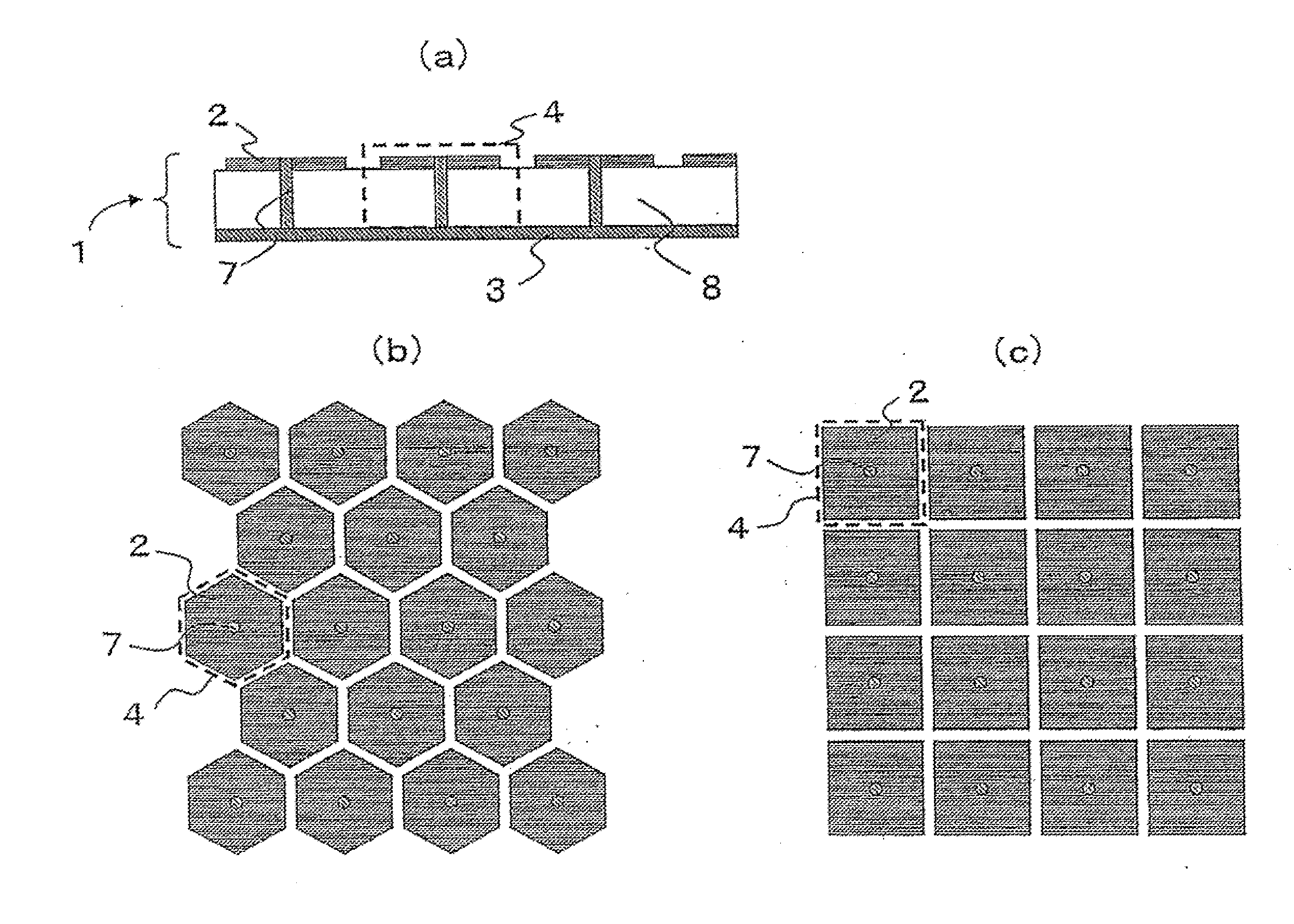
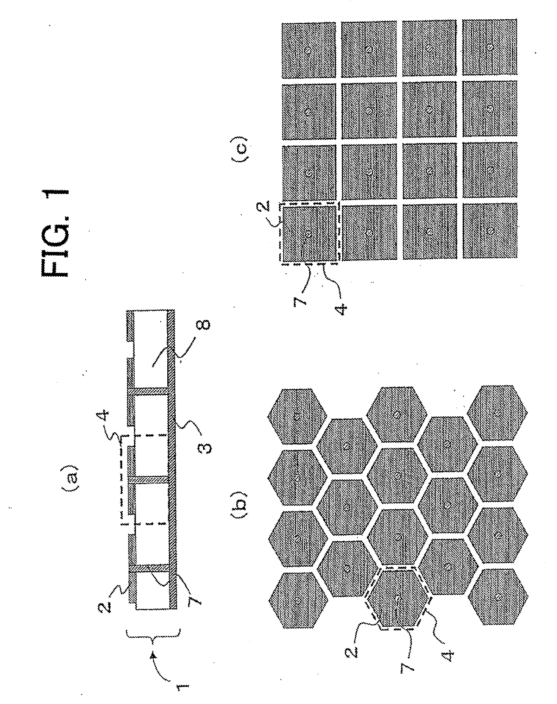
[0081]FIG. 7 shows a cross-sectional view of an electromagnetic band gap (EBG) device according to a first embodiment of the present invention. The EBG device 101 includes two conductor layers and a dielectric plate 108 that is sandwiched between the two conductor layers. The two conductor layers consist of a conductor layer that includes a periodic array of conductor pieces 102, and a conductor plane 103 that has openings 104 periodically formed. The openings 104 correspond to the periodic array of conductor pieces 102.
[0082]Island electrodes 105 and inductance elements 106 are arranged in the respective openings 104 of the conductor plane 103. The conductor plane 103, the planar inductance elements 106, and the island electrodes 105 are formed in the same conductor layer. The island electrodes 105 and the respective conductor pieces 102 are electrically connected by conductor posts 107.
[0083]The dielectric plate 108 is made of an epoxy resin substrate, a ceramic substrate, or the ...
second embodiment
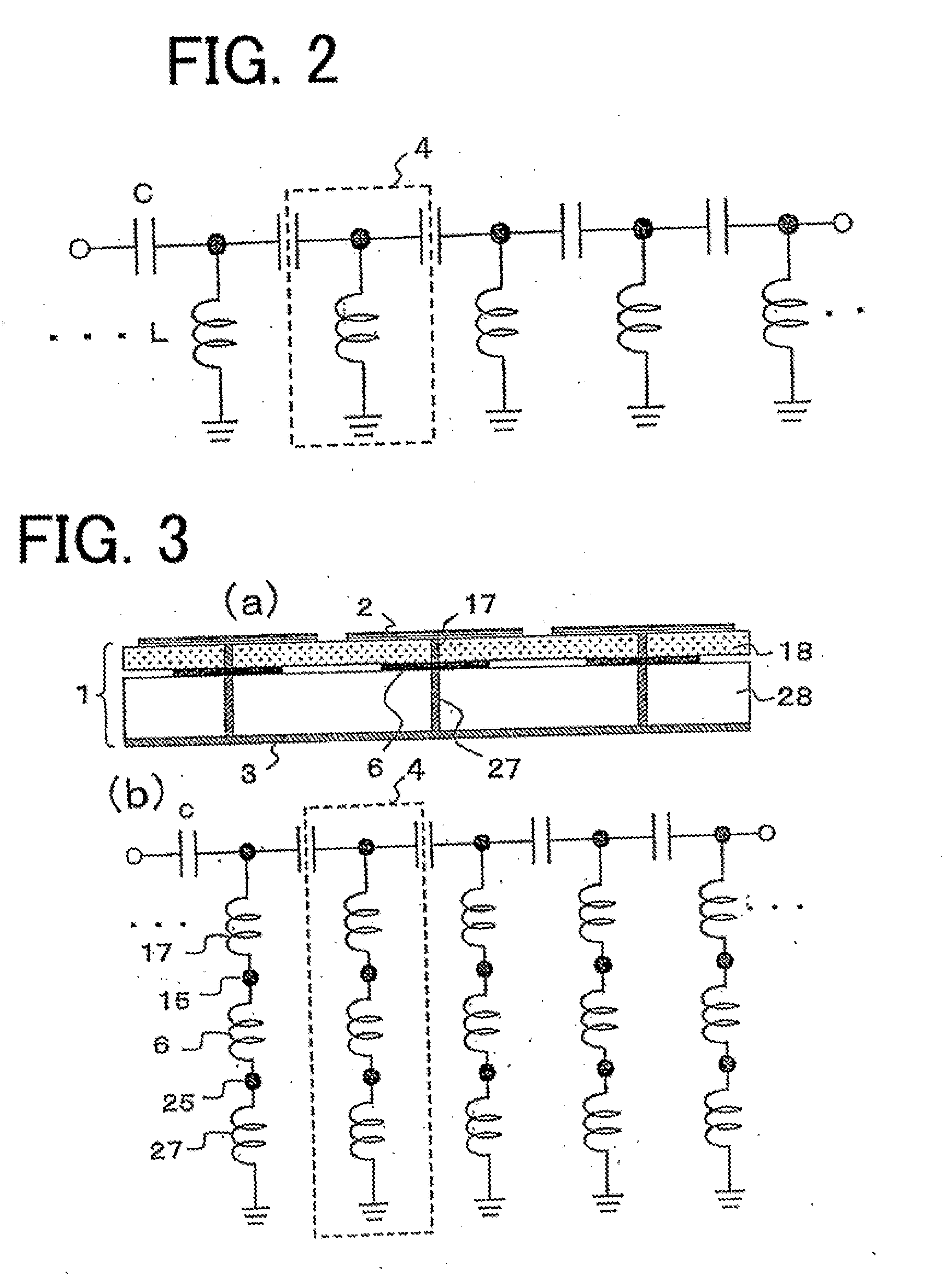
[0097]FIG. 14 is a sectional view showing a second embodiment of the present invention. In the present embodiment, an EBG device 201 includes three conductor layers. The three conductor layers consist of a conductor layer that constitutes a periodic array of conductor pieces 202, a conductor layer of a conductor plane 203 in which openings 204 are periodically formed, and a conductor layer in which planar inductance elements 206 are formed.
[0098]A first dielectric plate 218 is interposed between the conductor layer that constitutes the periodic array of conductor pieces 202 and the conductor plane 203. A second dielectric plate 228 is interposed between the conductor plane 203 and the layer in which the planar inductance elements 206 are formed. The conductor plane 203 is formed in the layer between the conductor layer in which the conductor pieces 202 are formed and the conductor layer in which the planar inductance elements 206 are formed. Island electrodes 205 are arranged in the...
third embodiment
[0103]As a structure for increasing the inductances of the planar inductance elements, the planar inductance elements may be covered with an insulating magnetic layer. FIGS. 16(a) and 16(b) show such a third embodiment of the present invention. FIG. 16(a) is a sectional view where the structure of covering the planar inductance elements with an insulating magnetic layer is applied to the embodiment of FIG. 1. In FIG. 16(a), the same parts as in FIG. 7 are designated by identical reference symbols.
[0104]FIG. 16(b) is a sectional view where the structure of covering the planar inductance elements with an insulating magnetic layer is applied to the embodiment of FIG. 14. In FIG. 16(b), the same parts as in FIG. 14 are designated by identical reference symbols.
[0105]In the structures according to the first embodiment of FIG. 7 and the second embodiment of FIG. 14, the planar inductance elements 106 and 206 can be formed in the surface conductor layer. As shown in FIG. 16(a), after the f...
PUM
 Abstract
Description
Claims
Application Information
 - R&D
- Intellectual Property
- Life Sciences
- Materials
- Tech Scout
- Unparalleled Data Quality
- Higher Quality Content
- 60% Fewer Hallucinations
Browse by: Latest US Patents, China's latest patents, Technical Efficacy Thesaurus, Application Domain, Technology Topic, Popular Technical Reports.
© 2025 PatSnap. All rights reserved.Legal|Privacy policy|Modern Slavery Act Transparency Statement|Sitemap|About US| Contact US: help@patsnap.com


