Power-supply-noise cancelling circuit and solid-state imaging device
a technology of power supply and noise cancelling circuit, which is applied in the direction of code conversion, television system, instruments, etc., can solve the problems of degrading resolution and unable to extract read levels
- Summary
- Abstract
- Description
- Claims
- Application Information
AI Technical Summary
Problems solved by technology
Method used
Image
Examples
first embodiment
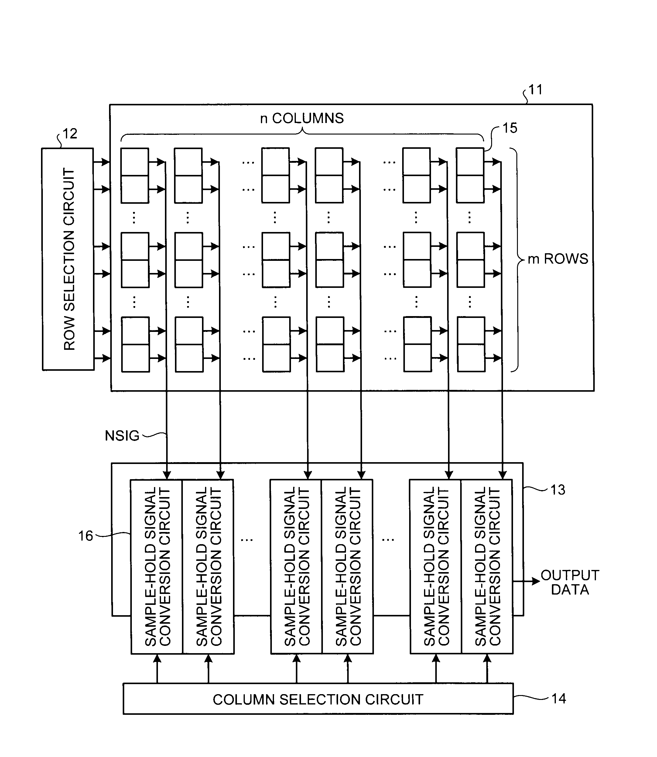
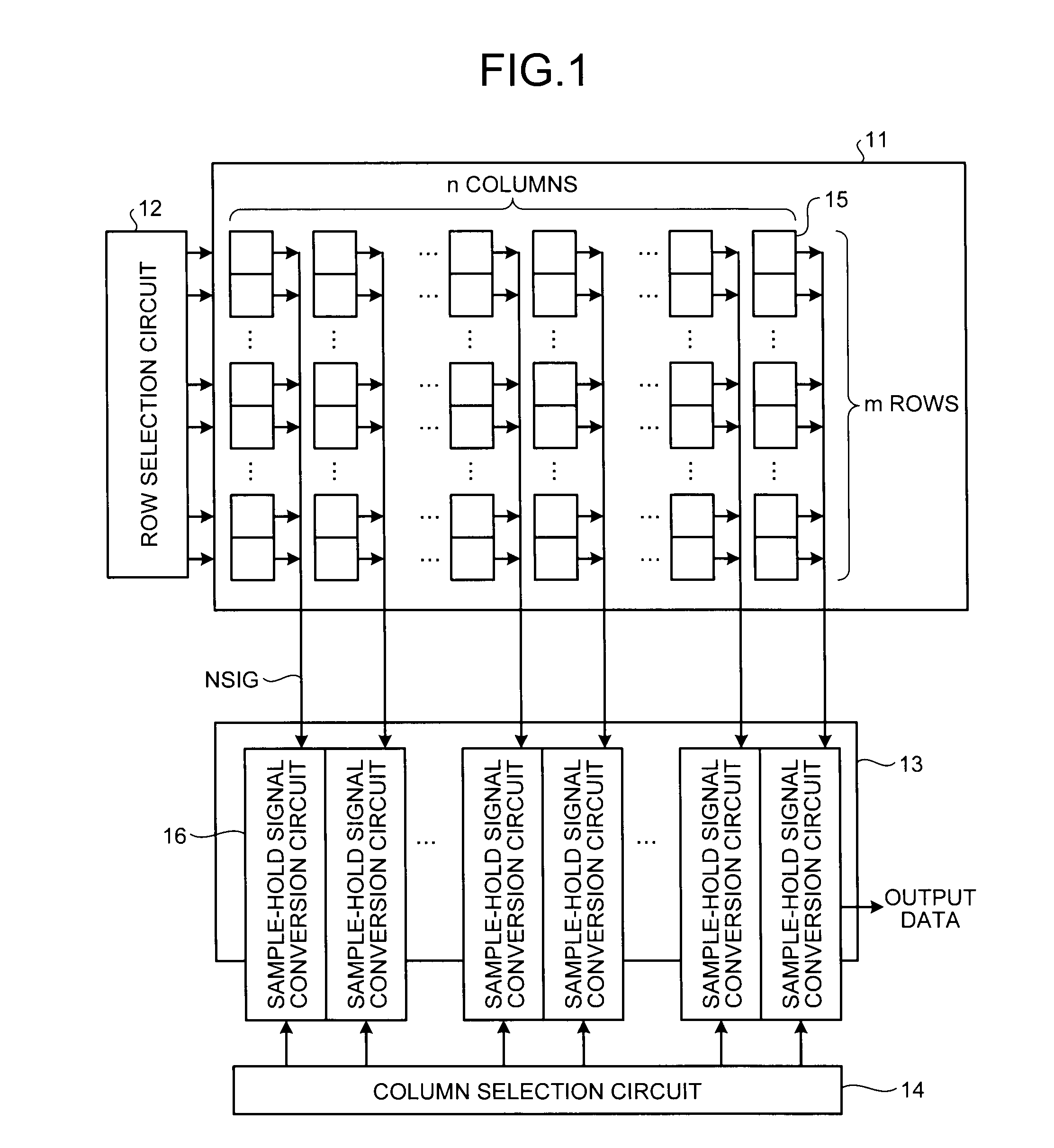
[0037]FIG. 1 is a block diagram of a general configuration of a CMOS image sensor to which a power-supply-noise cancelling circuit according to a first embodiment of the present invention is applied.
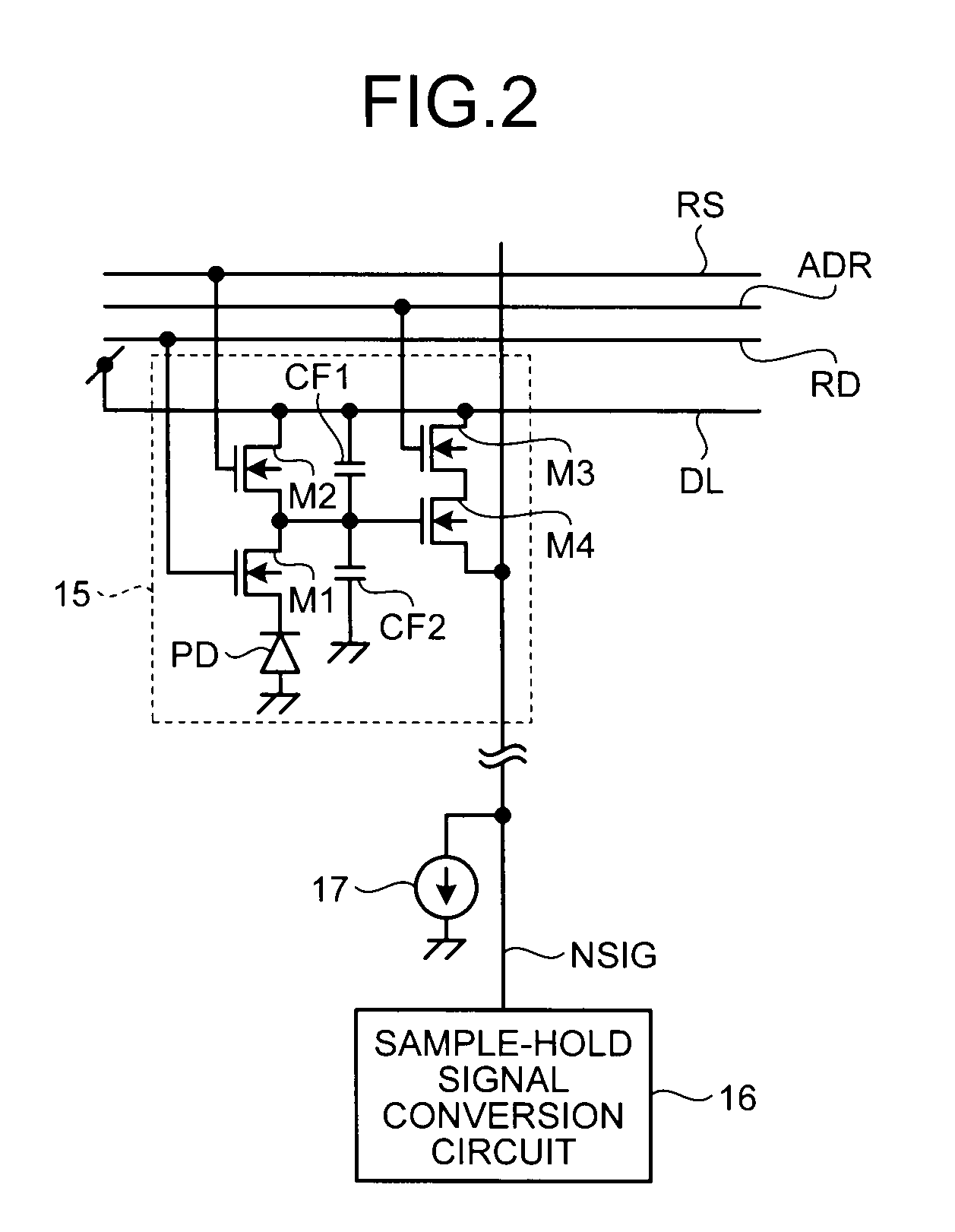
[0038]In FIG. 1, the CMOS image sensor includes a pixel array 11, a row selection circuit 12, a sample-hold signal conversion circuit group 13, and a column selection circuit 14. In the pixel array 11, pixels 15 that perform photoelectric conversion are arrayed in a matrix of m rows and n columns (m and n are integers equal to or larger than 1). The row selection circuit 12 is able to select a row in which the pixel 15 as a read target is arrayed. The column selection circuit 14 is able to select a column in which the pixel 15 as the read target is arrayed. In the sample-hold signal conversion circuit group 13, sample-hold signal conversion circuits 16 are arranged for respective columns of the array of the pixels 15. The sample-hold signal conversion circuits 16 are connected to each pi...
second embodiment
[0075]FIG. 5 is a block diagram of a general configuration of a power-supply-noise cancelling circuit applied to a sample-hold signal conversion circuit according to a second embodiment of the present invention.
[0076]In FIG. 5, the power-supply-noise cancelling circuit includes a power-supply-noise adding circuit 23′ instead of the power-supply-noise adding circuit 23 illustrated in FIG. 3, and further includes a register 26. The power-supply-noise adding circuit 23′ includes variable capacitance elements CH1 and CH2. One end of the variable capacitance element CH1 is connected to the power supply and one end of the variable capacitance element CH2 is connected to the ground. Furthermore, the other end of the variable capacitance element CH1 is connected to the amplifier reference voltage line NBIAS via the switch S4, and the other end of the variable capacitance element CH2 is connected to the amplifier reference voltage line NBIAS.
[0077]Furthermore, the register 26 is able to sele...
third embodiment
[0086]FIG. 8 is a block diagram of a general configuration of a power-supply-noise cancelling circuit applied to a sample-hold signal conversion circuit according to a third embodiment of the present invention.
[0087]In FIG. 8, the power-supply-noise cancelling circuit includes a power-supply-noise adding circuit 23″ instead of the power-supply-noise adding circuit 23′ illustrated in FIG. 5. The power-supply-noise adding circuit 23″ includes a buffer 27 in addition to the configuration of the power-supply-noise adding circuit 23′. The buffer 27 is disposed between the variable capacitance element CH2 and the differential amplifier AMP1.
[0088]FIG. 9 is a diagram illustrating an example of a circuit configuration of the power-supply-noise adding circuit illustrated in FIG. 8.
[0089]In FIG. 9, the power-supply-noise adding circuit 23″ illustrated in FIG. 8 includes the buffer 27 in addition to the configuration illustrated in FIG. 6. The buffer 27 is disposed between the switch SWk-1′ an...
PUM
 Abstract
Description
Claims
Application Information
 - R&D
- Intellectual Property
- Life Sciences
- Materials
- Tech Scout
- Unparalleled Data Quality
- Higher Quality Content
- 60% Fewer Hallucinations
Browse by: Latest US Patents, China's latest patents, Technical Efficacy Thesaurus, Application Domain, Technology Topic, Popular Technical Reports.
© 2025 PatSnap. All rights reserved.Legal|Privacy policy|Modern Slavery Act Transparency Statement|Sitemap|About US| Contact US: help@patsnap.com


