
Liquid crystal display and manufacturing method thereof

a technology of liquid crystal display and manufacturing method, which is applied in the field of liquid crystal display, can solve the problems of increasing affecting the performance of limited exposure, so as to improve the response speed against voltage, increase the luminance of the black display, and improve the effect of contras

Inactive Publication Date: 2010-10-07
SONY CORP
View PDF1 Cites 2 Cited by
  • Summary
  • Abstract
  • Description
  • Claims
  • Application Information

AI Technical Summary

Benefits of technology

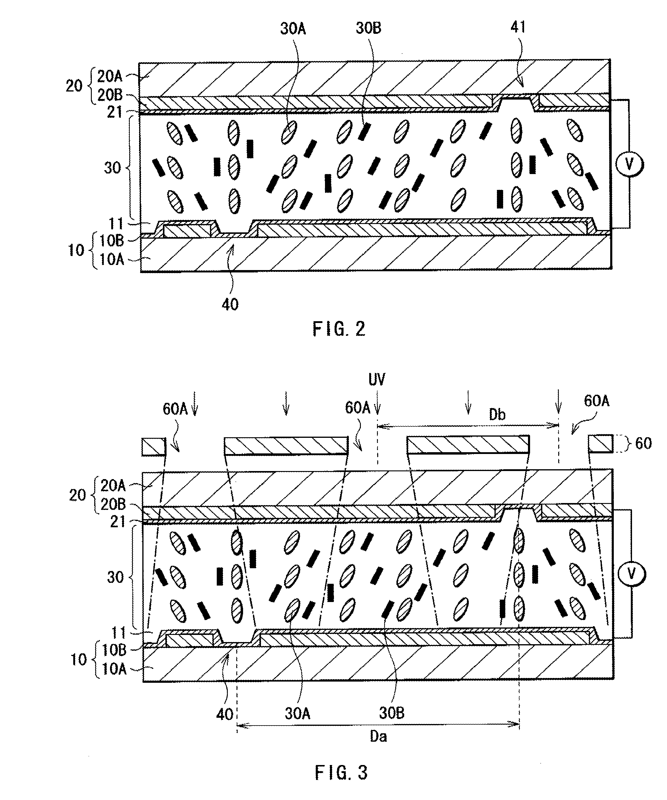
The present invention provides a method of manufacturing a liquid crystal display with improved response speed against voltage, while suppressing a drop in contrast. The method involves selectively imparting a pre-tilt angle to liquid crystal molecules in a region around the slits of the electrodes. By exposing the liquid crystal layer through a light shielding film with small openings, the pre-tilt angle can be efficiently imparted to the region with low response speed. The method does not require precise alignment between the mask for exposure and the pixel electrodes slits, and can be performed easily. The liquid crystal display made using this method has efficient response speed against voltage and suppressed contrast drop.

Problems solved by technology

This increases the luminance of the black display, leading to a drop in contrast.
However, in consideration of the spacing between the slits disposed in the upper and lower electrodes, it is extremely difficult to perform a limited exposure by selecting the pre-tilt region as described above.
This is because it is not easy to make precise alignment between the opening position of a mask for selective exposure and the slit position of the electrodes.

Method used


Image

  • Liquid crystal display and manufacturing method thereof
  • Liquid crystal display and manufacturing method thereof
  • Liquid crystal display and manufacturing method thereof

Examples


Embodiment Construction

[0032]Preferred embodiments of the present invention will now be described in detail with reference to the accompanying drawings.

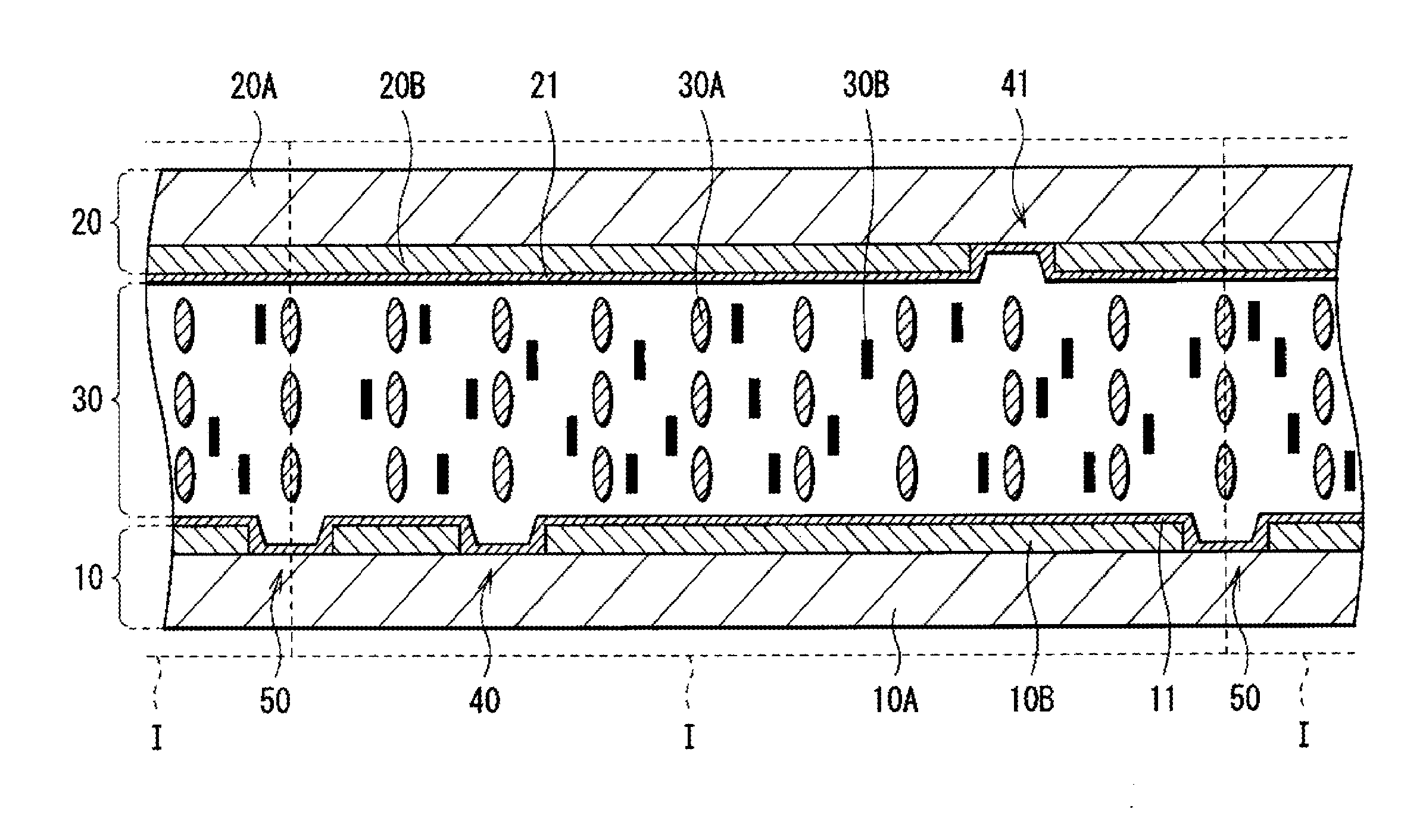
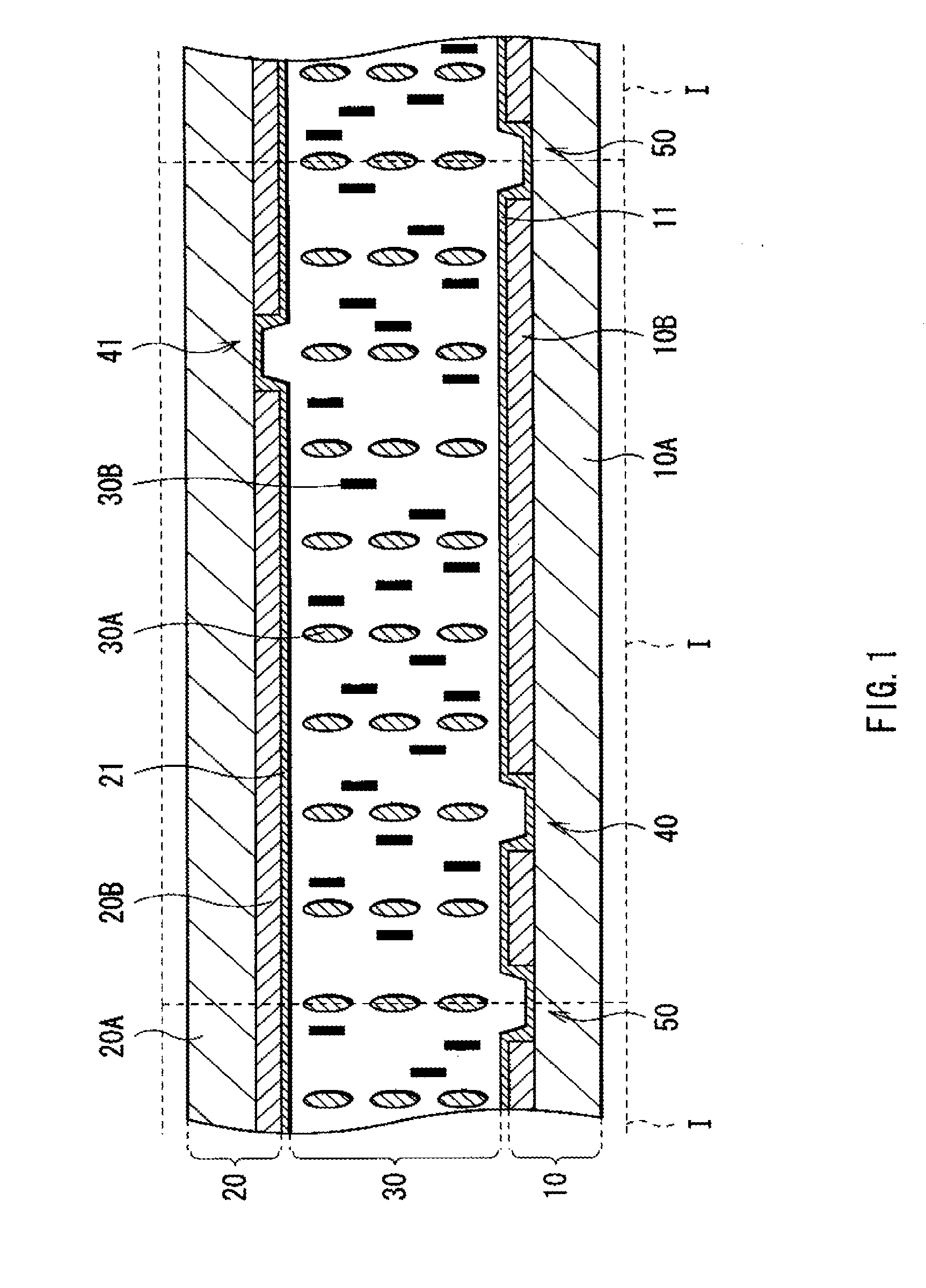
[0033]FIGS. 1 to 4 are cross-sectional views schematically illustrating the manufacturing steps of a liquid crystal panel according to a preferred embodiment of the present invention. The method of manufacturing a liquid crystal display includes the step of forming electrodes having predetermined slit parts on surfaces of a pair of boards, respectively, and then sealing a liquid crystal layer between the boards; and the step of exposing the liquid crystal layer through a predetermined light shielding film, under an applied voltage. This method is for manufacturing a liquid crystal panel where a plurality of pixels are formed between the boards, as shown in FIG. 1. For sake of simplicity, FIGS. 2 and 3 show only a region I (a pixel) in FIG. 1. In FIGS. 1 to 4, specific configurations of each board are omitted.

[0034]Firstly, as shown in FIG. 1, a TFT (thin f...


PUM

PropertyMeasurementUnit
voltageaaaaaaaaaa
shapeaaaaaaaaaa
voltageaaaaaaaaaa

Abstract

A liquid crystal display including a couple of substrates facing each other and pixel electrodes formed on inside surfaces of the couple of substrates, each of the pixel electrodes has gaps. A liquid crystal layer is sealed between the couple of substrates with the pixel electrodes formed and the gaps are alternately disposed to form a staggered arrangement between the pair of pixel electrodes. The liquid crystal layer has pre-tilt regions where liquid crystal molecules are tilted. In these regions, the spacing between adjacent pre-tilt regions is smaller than spacing in the substrate surface direction between the gap of a pixel electrode on one substrate and the gap of a pixel electrode on the other substrate.

Description

CROSS-REFERENCE TO RELATED APPLICATIONS[0001]This application is a continuation of U.S. application Ser. No. 11 / 939,255, entitled “LIQUID CRYSTAL DISPLAY AND MANUFACTURING METHOD THEREOF,” filed on Nov. 13, 2007, the entirety of which is incorporated herein by reference to the extent permitted by law. The present invention claims priority to Japanese Patent Application No. 2006-309515, filed Nov. 15, 2006, the entirety of which is also incorporated herein by reference to the extent permitted by law.[0002]The following identified U.S. patent applications are also relied upon and are incorporated by reference in this application:BACKGROUND OF THE INVENTION[0003]1. Field of the Invention[0004]The present invention relates to a liquid crystal display having a macromolecular dispersive liquid crystal layer containing a curing material, as well as a method of manufacturing the liquid crystal display.[0005]2. Description of the Related Art[0006]Recently, liquid crystal displays have been o...

Claims


Application Information

Patent Timeline
Patent Type & Authority Applications(United States)
IPC IPC(8): G02F1/1339
CPCG02F1/133707G02F2001/13712G02F2001/134318G02F1/134309G02F1/134318G02F1/13712G02F1/1343G02F1/1335
Inventor MIZUKI, MASAHIKOKAMADA, TSUYOSHI
Owner SONY CORP
Learn More