
Memory cell array biasing method and a semiconductor memory device

a memory cell array and biasing technology, applied in the field of semiconductor memory devices, can solve the problems of limited number of unit cells connected to the word lines wlb>0/b>, wlb>1/b>, wlb>2/b>, and it is difficult to increase perform stable sensing. , to achieve the effect of stable sensing and increasing the operating speed of the semiconductor memory devi

Active Publication Date: 2010-09-30
SAMSUNG ELECTRONICS CO LTD
View PDF4 Cites 0 Cited by
  • Summary
  • Abstract
  • Description
  • Claims
  • Application Information

AI Technical Summary

Benefits of technology

[0016]A semiconductor memory device and a data writing method are provided that prevent current from flowing from a selected bit line to a non-selected word line by maintaining a constant voltage in the non-selected word line, thereby enabling stable sensing and increasing the operating speed of the semiconductor memory device.

Problems solved by technology

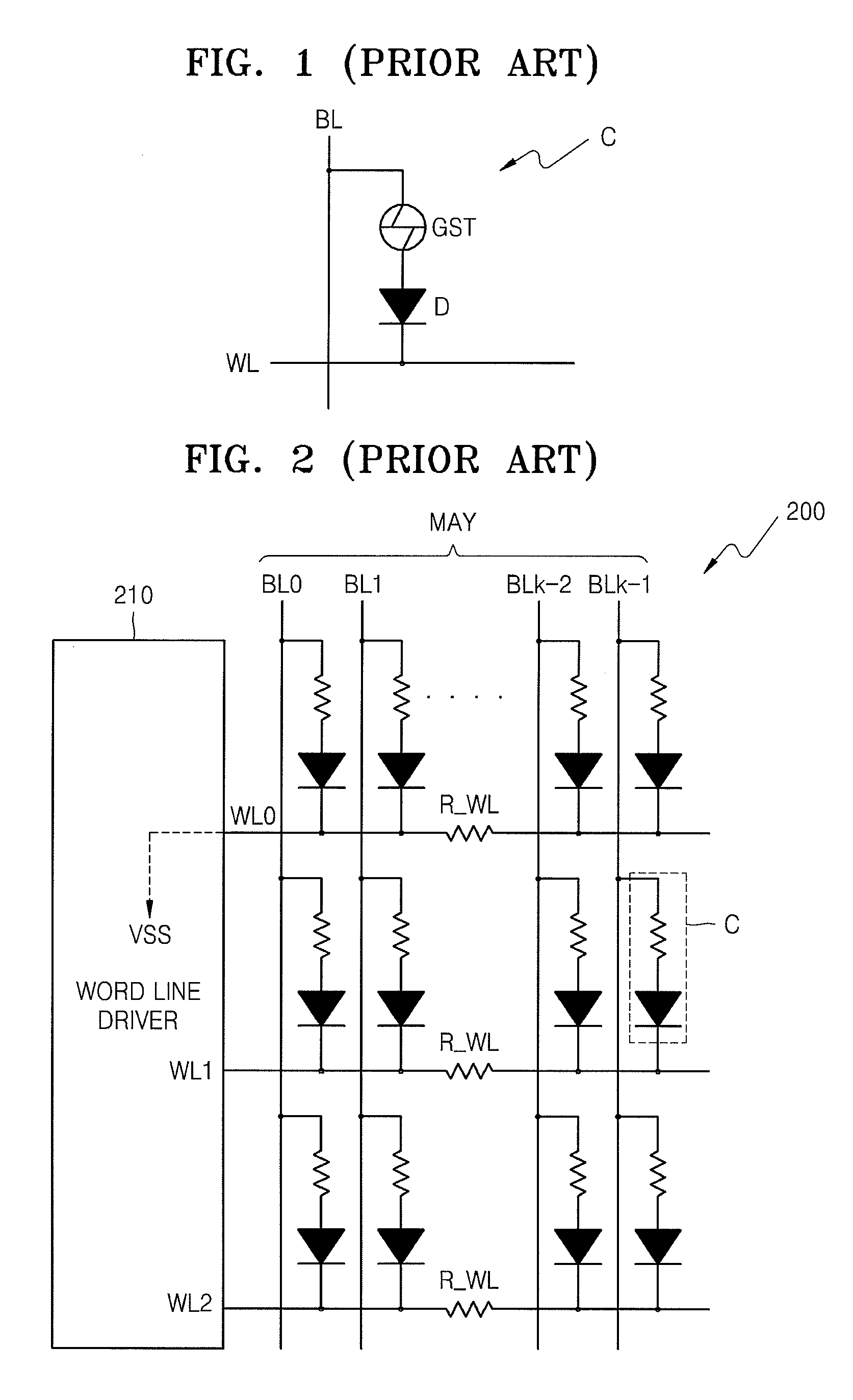
Because the word lines WL0, WL1, and WL2 have a high resistance, however, the number of unit cells connected to the word lines WL0, WL1, and WL2 is limited.
Because current may flow through unselected word lines that are floating, it is difficult to increase the operating speed of the semiconductor memory device and perform stable sensing.

Method used


Image

  • Memory cell array biasing method and a semiconductor memory device
  • Memory cell array biasing method and a semiconductor memory device
  • Memory cell array biasing method and a semiconductor memory device

Examples


Embodiment Construction

[0037]The present invention will now be described more fully with reference to the accompanying drawings, in which exemplary embodiments of the invention are shown. Like reference numerals represent like elements throughout the drawings.

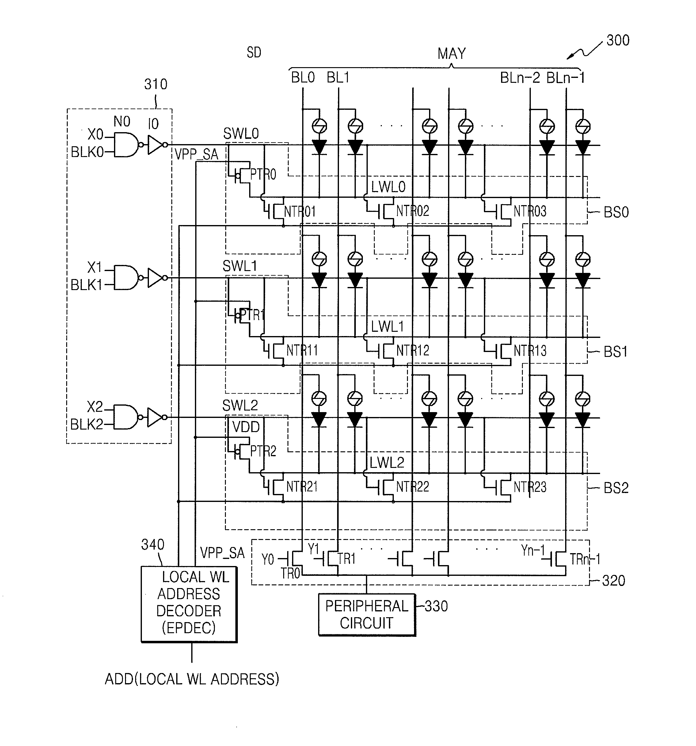
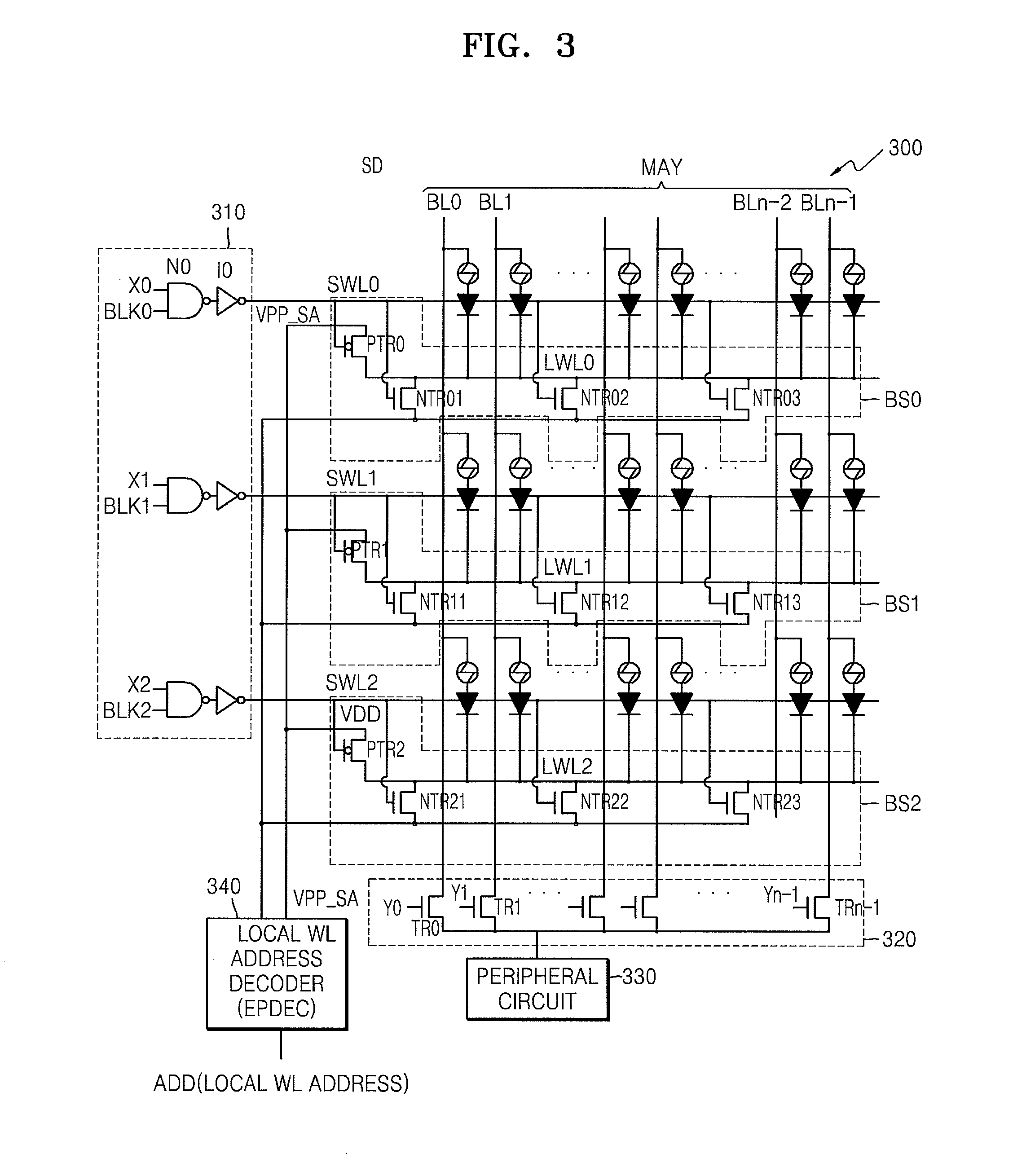
[0038]FIG. 3 illustrates a semiconductor memory device 300 according to an exemplary embodiment of the present invention. Referring to FIG. 3, the semiconductor memory device 300 includes a memory cell array MAY, bias circuits BS0, BS1, and BS2, and a word line driver 310. The semiconductor memory device 300 is a PRAM, which includes a memory cell having a phase change material, e.g., GST, connected to a first line, and a diode connected between the phase change material and a second line. The PRAM may be similar to or the same as that shown in FIG. 1.

[0039]As shown in FIG. 3, the semiconductor memory device 300 is connected to a peripheral circuit 330, a column decoder 320, and a local word time address decoder 340. The peripheral circuit 330 may co...


PUM


Abstract

A method of biasing a memory cell array during a data writing operation and a semiconductor memory device, in which the semiconductor memory device includes: a memory cell array including a plurality of memory cells in which a first terminal of a memory cell is connected to a corresponding first line of a plurality of first lines and a second terminal of the memory cell is connected to a corresponding second line of a plurality of second lines; a bias circuit for biasing a selected second line of the second lines to a reference voltage and a non-selected second line to a first voltage; and a local word line address decoder applying the reference voltage or a pumping voltage corresponding to the first voltage to the bias circuit.

Description

CROSS-REFERENCE TO RELATED APPLICATIONS[0001]This application is a continuation-in-part of application Ser. No. 11 / 969,326 filed Jan. 4, 2008, which is a continuation-in-part of application Ser. No. 11 / 327,967, filed Jan. 9, 2006 now U.S. Pat. No. 7,317,655, which claims priority to Korean Patent Application No. 10-2005-0006581, filed on Jan. 25, 2005, in the Korean Intellectual Property Office, the disclosures of which are incorporated by reference herein in their entirety.BACKGROUND OF THE INVENTION[0002]1. Technical Field[0003]The present disclosure relates to a semiconductor memory device, and more particularly, to a semiconductor memory device and a data writing method for controlling a biasing level of a memory cell array.[0004]2. Discussion of Related Art[0005]Phase change random access memories (PRAMs) are nonvolatile memory devices that store data using a phase change material, e.g., Ge—Sb—Te (GST), whose resistance changes in accordance with a phase transition due to a cha...

Claims


Application Information

Patent Timeline
Patent Type & Authority Applications(United States)
IPC IPC(8): G11C11/00G11C8/08
CPCG11C8/08G11C13/0004G11C13/0023G11C13/0028G11C2213/72G11C13/004G11C13/0069G11C2013/009G11C13/0038
Inventor CHO, BEAK-HYUNGKIM, DO-EUNGKWAK, CHOONG-KEUNKANG, SANG-BEOMCHO, WOO-YEONGOH, HYUNG-ROK
Owner SAMSUNG ELECTRONICS CO LTD
Learn More