
Active device array substrate and method for fabricating the same

a technology of active devices and substrates, which is applied in the field of display arrays, can solve the problems of limited flattening capability of crts, poor photoelectric conversion efficiency of p-i-n photosensors manufactured by ltps technology, and poor quantum effect of p-i-n photosensors, etc., and achieves enhanced photosensor sensitivity, high compatibility, and reduced process costs

Active Publication Date: 2010-09-16
AU OPTRONICS CORP
View PDF7 Cites 11 Cited by
  • Summary
  • Abstract
  • Description
  • Claims
  • Application Information

AI Technical Summary

Benefits of technology

"The present invention provides a method for fabricating an active device array substrate incorporating a photo sensor without requiring additional photolithography and etching processes. This method allows for more accurate sensitivity and low-cost fabrication. The method includes steps of forming a first patterned semiconductor layer, a gate insulator, a first patterned conductive layer, and a first dielectric layer on a substrate. A second patterned conductive layer and a second patterned semiconductor layer are then sequentially formed on the first dielectric layer. A second conductive layer and a second semiconductor layer are patterned to form the bottom electrode and the active layer. The second patterned conductive layer is electrically connected to the first patterned semiconductor layer through a portion of the second contact holes and the second patterned conductive layer. The second patterned semiconductor layer may also include dummy semiconductor layers. Overall, this method simplifies the fabrication process and improves the sensitivity of the photo sensor."

Problems solved by technology

However, the rise of “environmental protection” awareness is against the CRTs due to the CRTs' disadvantages including high power consumption and high radiation, and the limited flattening capability of the CRTs is against the market demands for light, thin, short, small, compact, and power-saving displays.
However, due to the limitation of the process, the p-i-n photo-sensors manufactured by the LTPS technology have a poor quantum effect (i.e. photoelectric conversion efficiency) because of an insufficient thickness of the poly-silicon thin film.
In addition, the light from a backlight source directly irradiates the p-i-n photo sensor through the glass substrate and thus affects the photosensitive characteristics of the p-i-n photo sensor, reduces a signal to noise ratio (SNR) of a photosensitive signal, and causes distortion of measurement results.
In other words, a photosensitive material serving as the active layer in the photo sensor has the problem that, even though a voltage is not applied to electrodes on two sides of the photosensitive material, as long as the photosensitive material is irradiated by light, the reliability performance of the photo sensor is affected due to the attenuation of photo current of the photo sensor.
Therefore, the fabricating process can not be curtailed to reduce the process cost, which results in lowering the competitiveness of the product.

Method used


Image

  • Active device array substrate and method for fabricating the same
  • Active device array substrate and method for fabricating the same
  • Active device array substrate and method for fabricating the same

Examples


first embodiment

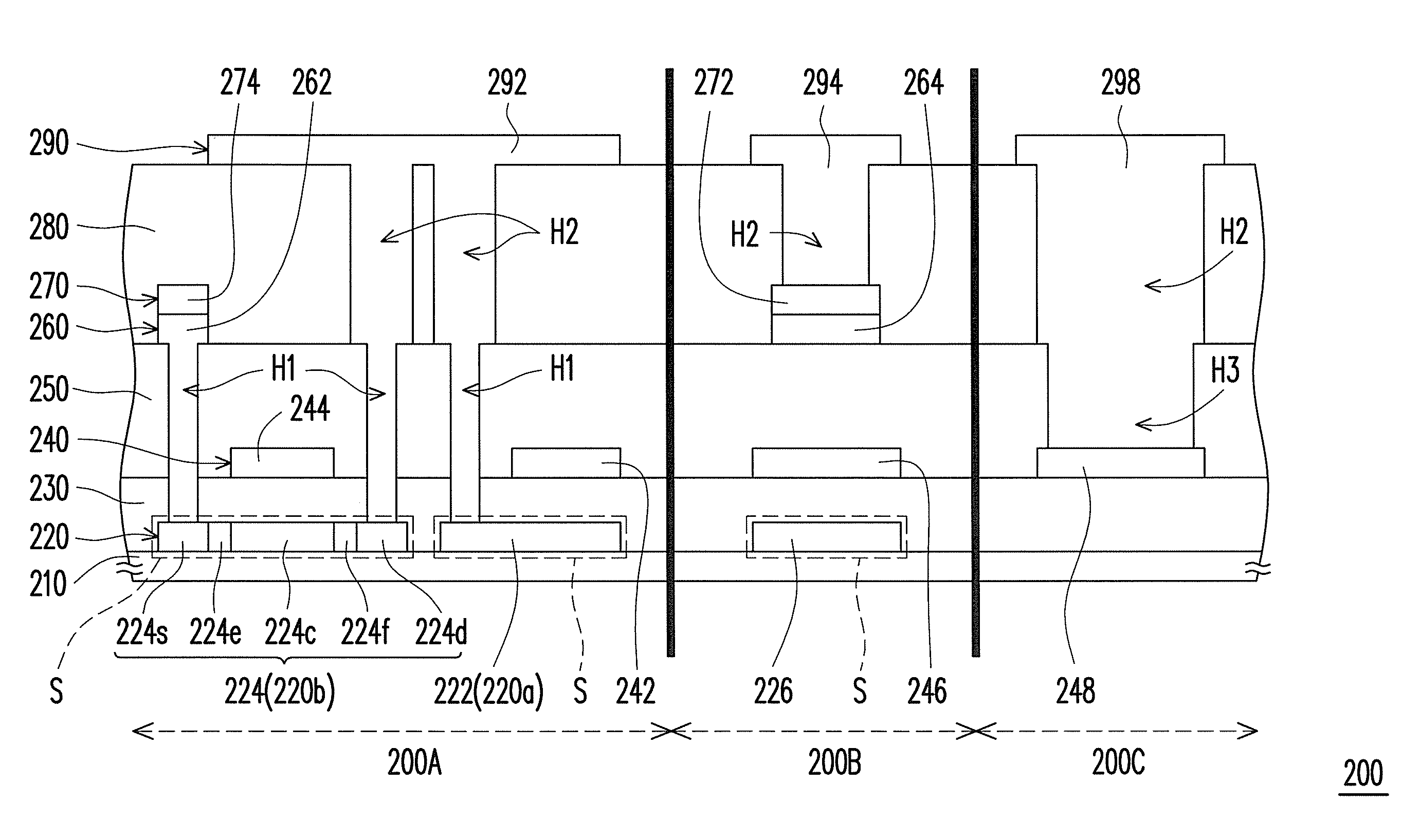
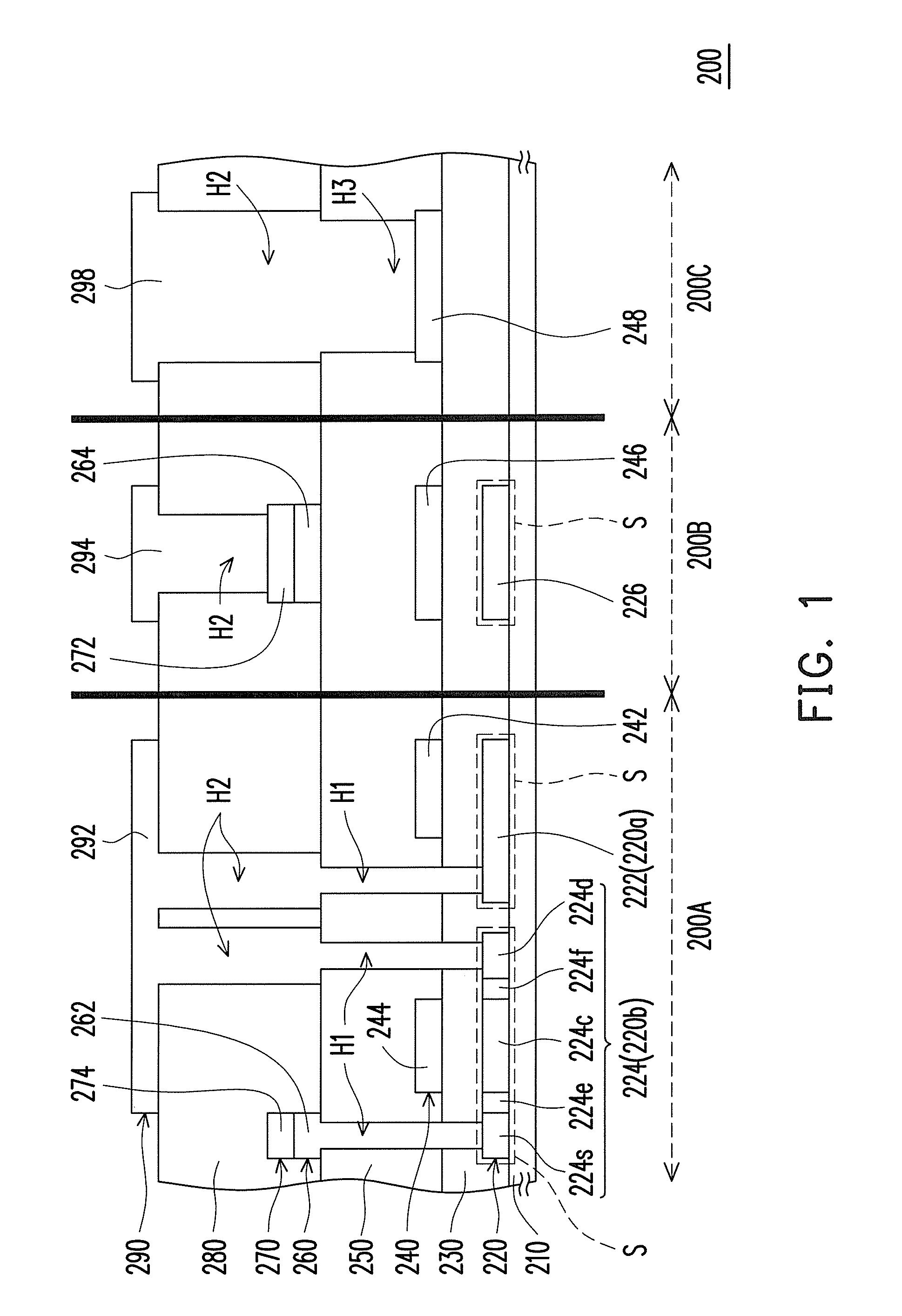
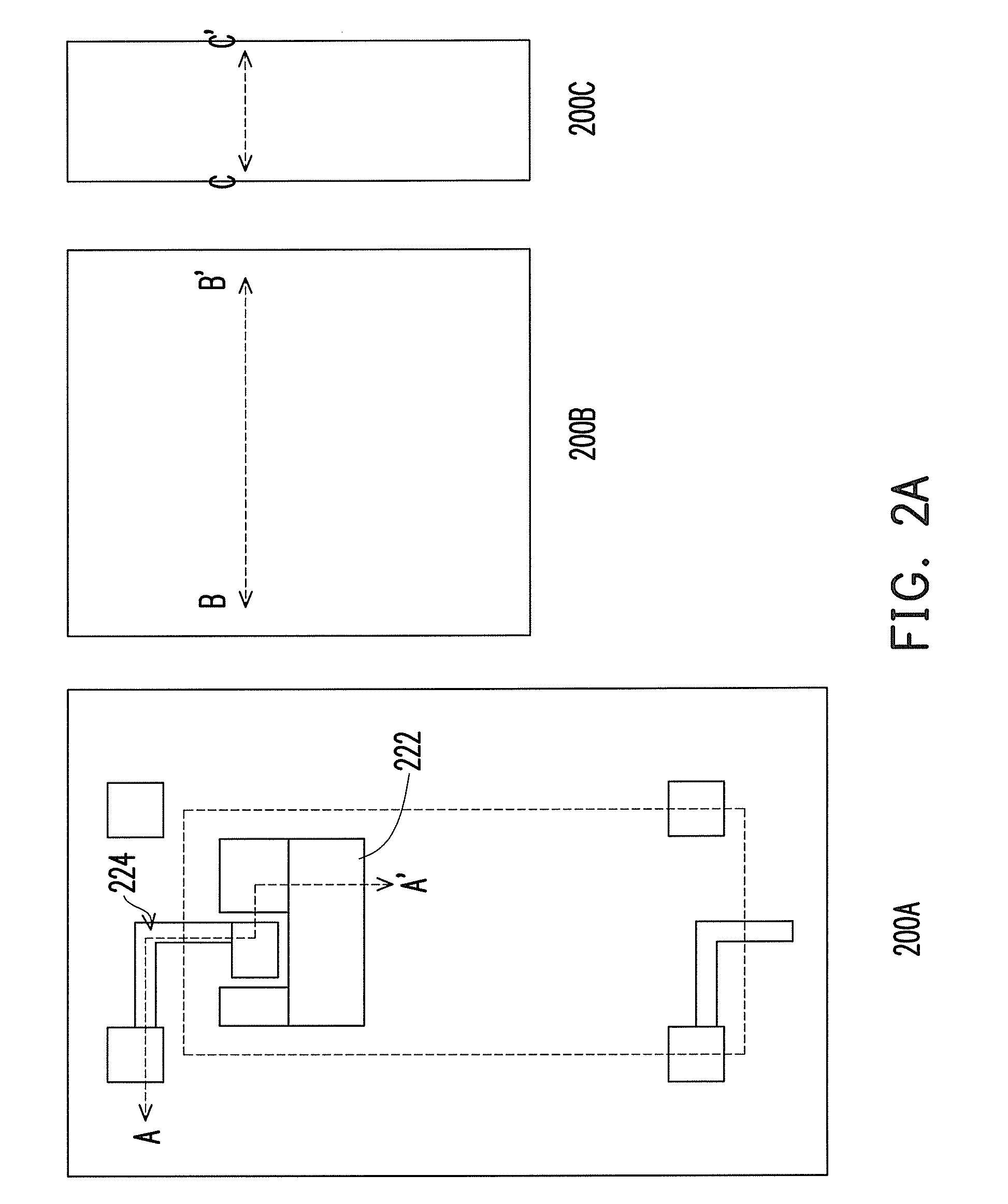
[0085]FIG. 1 shows an active device array substrate according to one embodiment of the present invention. For the purpose of simplification, elements which may be plural may be shown as singular in FIG. 1. Furthermore, in order to facilitate the illustration, the active device array substrate is divided into a pixel region 200A, a sensing region 200B, and a pad region 200C, as shown in FIG. 1. The pixel region 200A has an active device therein for controlling displaying status. According to the present embodiment, the active device in the pixel region 200A can incorporate a storage capacitor to achieve desired display performance.

[0086]Referring to FIG. 1, the active device array substrate 200 includes a substrate 210, a first patterned semiconductor layer 220, a gate insulator 230, a first patterned conductive layer 240, a first dielectric layer 250, a second patterned conductive layer 260, a second patterned semiconductor layer 270, a second dielectric layer 280, and a third patte...

second embodiment

[0107]FIG. 3 illustrates an active device array substrate according to a second embodiment of the present invention. Referring to FIG. 3, an active device array substrate 300 of the present embodiment is similar to the active device array substrate 200 of the first embodiment. Compared with the first embodiment, in the active device array substrate 300 of the present embodiment, the pixel electrode 292 in the pixel region 200A is electrically connected to the first patterned semiconductor layer 220 in an indirect manner through the first patterned conductive layer 240 and the second patterned conductive layer 260, for example.

[0108]In detail, compared with the first embodiment, the first patterned conductive layer 240 of the active device array substrate 300 further includes a bridge electrode 249 disposed in the pixel region 200A. Meanwhile, the contact conductors 262 of the active device array substrate 300 are filled into the first contact holes H1 and respectively in contact wit...

third embodiment

[0116]FIG. 5 illustrates an active device array substrate according to a third embodiment of the present invention. Referring to FIG. 5, an active device array substrate 400 of the present embodiment is similar to the active device array substrates 200 and 300 of the foregoing embodiments. However, compared with the active device array substrates 200 and 300 of the foregoing embodiments, in the active device array substrate 400, the third patterned conductive layer 290, serving as the pixel electrode 292, in the pixel region 200A is electrically connected to the first patterned semiconductor layer 200 through a portion of the second contact holes H2 and the second patterned conductive layer 260. Moreover, according to the present embodiment, the second patterned semiconductor layer 270 further includes a plurality of dummy semiconductor layer 274 disposed on the contact conductor 262, wherein the sizes of a portion of the dummy semiconductor layers 274 are, for example, substantiall...


PUM


Abstract

A method for fabricating an active device array substrate is provided. A first patterned semiconductor layer, a gate insulator, a first patterned conductive layer and a first dielectric layer is sequentially formed on a substrate. First contact holes exposing the first patterned semiconductor layer are formed in the first dielectric layer and the gate insulator. A second patterned conductive layer and a second patterned semiconductor layer disposed thereon are simultaneously formed on the first dielectric layer. The second conductive layer includes contact conductors and a bottom electrode. The second patterned semiconductor layer includes an active layer. A second dielectric layer having second contact holes is formed on the first dielectric layer, wherein a portion of the second contact holes exposes the active layer. A third patterned conductive layer electrically connected to the active layer through a portion of the second contact holes is formed on the second dielectric layer.

Description

CROSS-REFERENCE TO RELATED APPLICATION[0001]This application claims the priority benefit of Taiwan application serial no. 98108435, filed on Mar. 16, 2009. The entirety of the above-mentioned patent application is hereby incorporated by reference herein and made a part of specification.BACKGROUND OF THE INVENTION[0002]1. Field of the Invention[0003]The present invention relates to a display array and a method for fabricating the same, and in particular, to an active device array substrate and a method for fabricating the same.[0004]2. Description of Related Art[0005]With a rapid progress in science and technology, a demand for displays is increasing along with an advancement of display technology. Conventionally, since cathode ray tubes (CRTs) are fully developed and have extraordinary display quality, the CRTs have played a dominant role in the display market for years. However, the rise of “environmental protection” awareness is against the CRTs due to the CRTs' disadvantages incl...

Claims


Application Information

Patent Timeline
Patent Type & Authority Applications(United States)
IPC IPC(8): H01L27/085H01L21/8232H01L21/336
CPCH01L27/1214H01L27/14609H01L27/14692H01L27/14645H01L27/14623H01L27/1288
Inventor SUN, MING-WEILI, CHEN-YUEHCHEN, YU-CHENGPENG, CHIA-TIEN
Owner AU OPTRONICS CORP
Learn More