Pixel structure and driving method thereof
a liquid crystal display and pixel structure technology, applied in the field of pixel structure of wide view angle liquid crystal display, can solve the problems of image sticking, increased manufacturing cost, and double the number of gate lines or data lines used in this pixel structur
- Summary
- Abstract
- Description
- Claims
- Application Information
AI Technical Summary
Problems solved by technology
Method used
Image
Examples
Embodiment Construction
[0024]It should be noticed that, wherever possible, the same reference numbers will be used throughout the drawings to refer to the same or like parts.
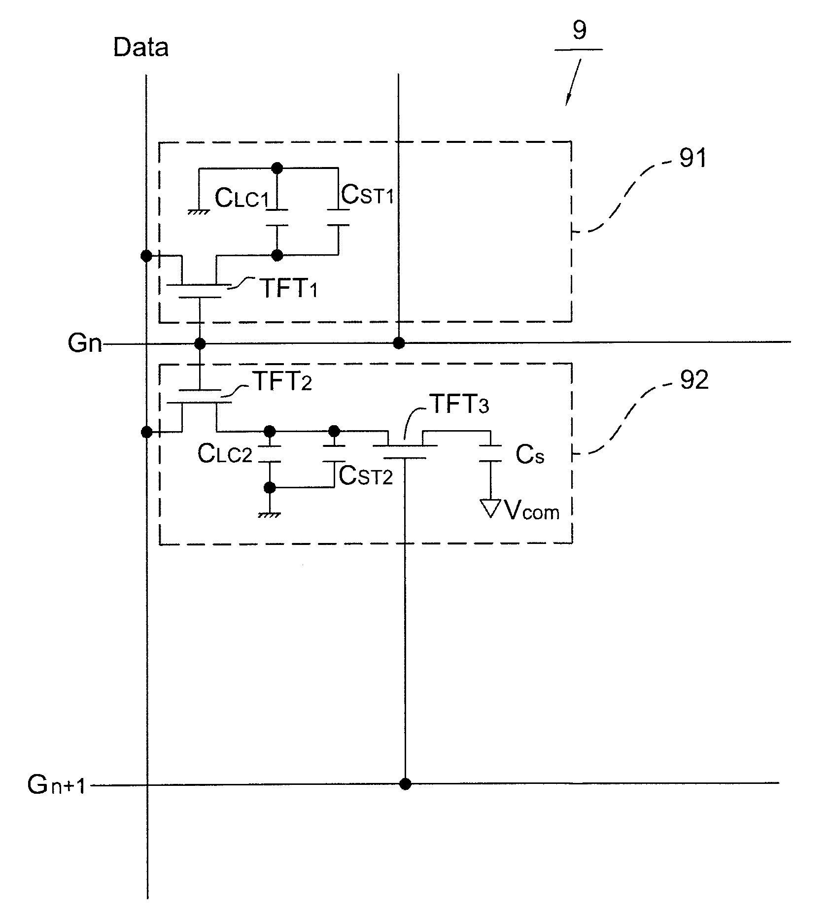
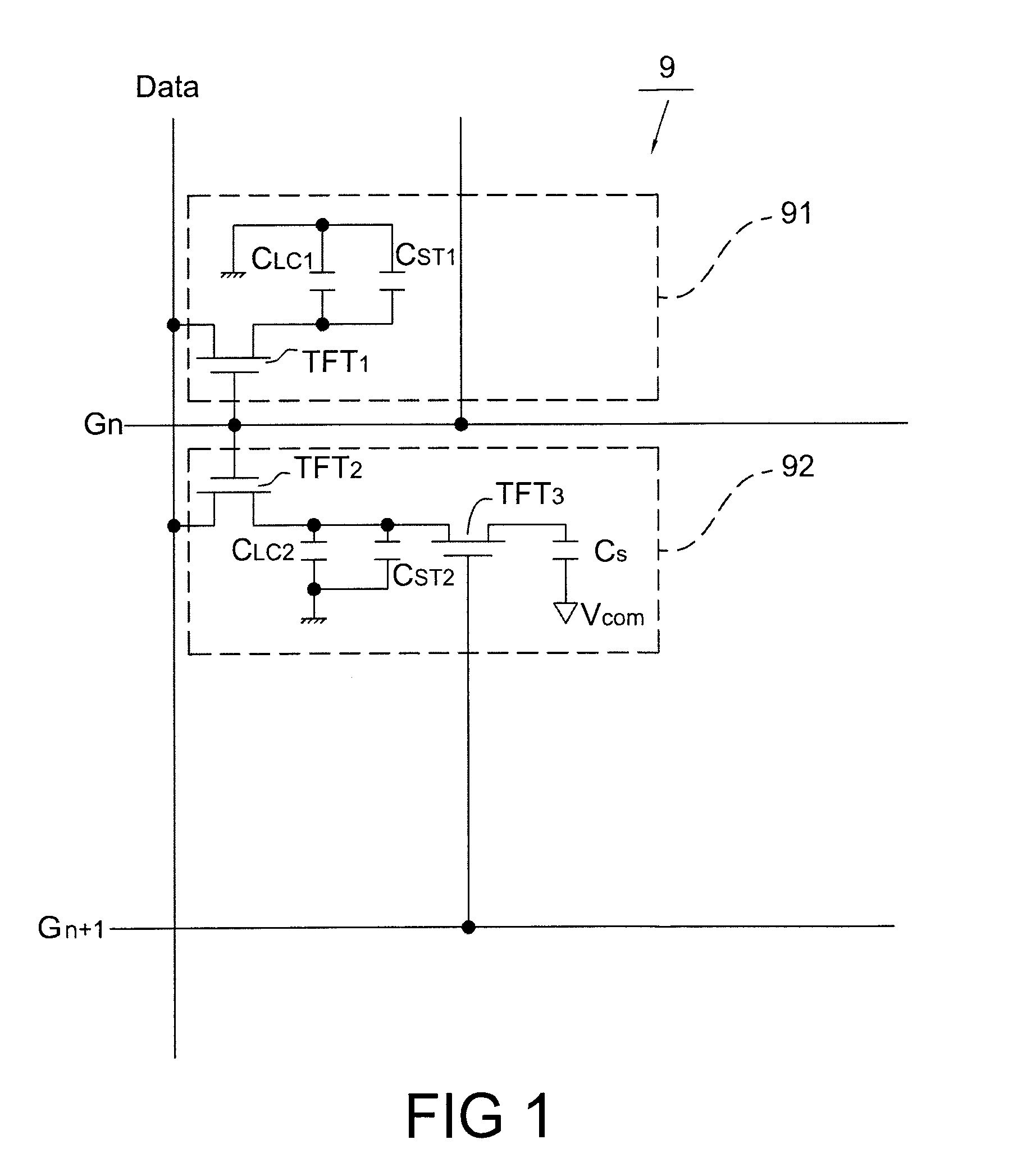
[0025]Please refer to FIG. 4, it shows a pixel structure 1 according to an embodiment of the present invention. The pixel structure 1 includes a first gate line Gn, a data line Data, a first sub-pixel A and a second sub-pixel B, wherein the data line Data is configured to provide gray level voltages to a row of pixel structures during display periods. In this embodiment, the first sub-pixel A and the second sub-pixel B may have different gray level voltages during display periods of the pixel structure 1 by means of charge sharing. It should be understood that, the pixel structure 1 shown in FIG. 4 only shows the components for illustrating the present invention and omits other components.
[0026]The first sub-pixel A includes a first switching transistor TFT1, a first liquid crystal capacitor CLCA and a first storage capacitor CSTA. Th...
PUM
 Abstract
Description
Claims
Application Information
 - R&D
- Intellectual Property
- Life Sciences
- Materials
- Tech Scout
- Unparalleled Data Quality
- Higher Quality Content
- 60% Fewer Hallucinations
Browse by: Latest US Patents, China's latest patents, Technical Efficacy Thesaurus, Application Domain, Technology Topic, Popular Technical Reports.
© 2025 PatSnap. All rights reserved.Legal|Privacy policy|Modern Slavery Act Transparency Statement|Sitemap|About US| Contact US: help@patsnap.com


