
Display device

a technology of a display device and a display screen, which is applied in the field of display devices, can solve the problems of requiring mechanical manipulation, i.e. the removal of the film, and the inefficiency of the display in its use of light, and achieves the effect of reducing the resolution of the side image and high degree of visually confusing information

Active Publication Date: 2010-08-26
SHARP KK
View PDF19 Cites 22 Cited by
  • Summary
  • Abstract
  • Description
  • Claims
  • Application Information

AI Technical Summary

Benefits of technology

[0062]The display device may comprise means for increasing the non-linearity of the off-axis luminance to on-axis luminance relationship.
[0065]An embodiment of the present invention provides a liquid crystal display with switchable privacy function. In the public mode, the display operates in a substantially unaltered manner from a standard LCD, in that for each frame of the video displayed, data constituting a single image is supplied to the display control electronics, the control electronics then output a series of signal voltages and timing signals to the active-matrix array of the display, and these voltages reorient the liquid crystal director within each pixel in such a way that the required amount of light is transmitted by each pixel through the display polarisers to cause the image to be displayed.
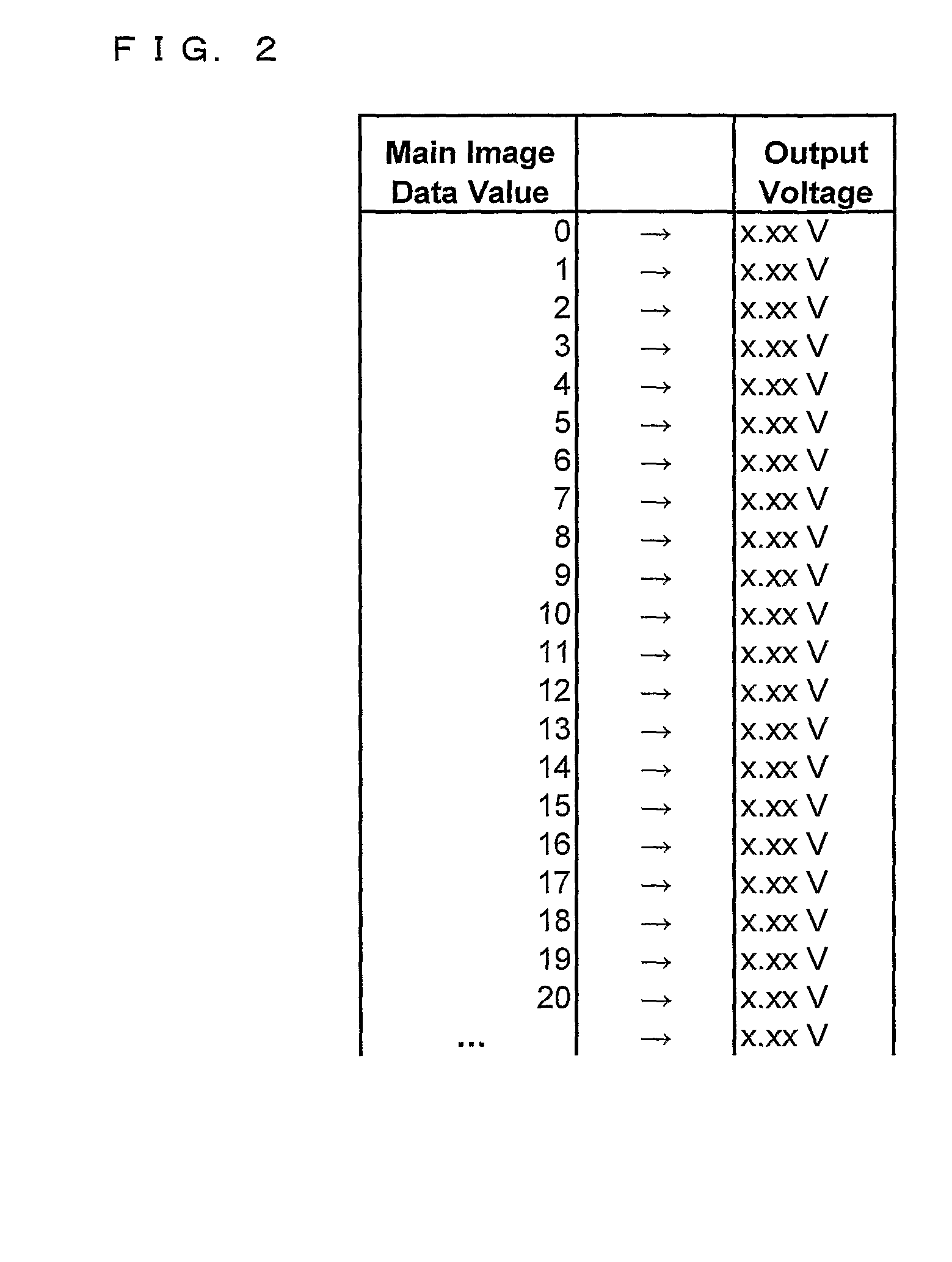
[0068]An embodiment of the present invention disclosed herein constitutes an LCD display with control electronics modified from the standard in order to allow it to output signal voltages which are dependent on one image in the public mode and two images in the private mode. It also constitutes specific relationships between the output signal voltages and the two input images which result in the main image being observed by the on-axis viewer with image quality as close as possible to that as would be observed if the main image were displayed in the public mode, and the side image simultaneously being observed by the off-axis viewer with optimal obscuring or degrading effect on the main image.

Problems solved by technology

The principal limitation of such films is that they require mechanical manipulation, i.e. removal of the film, to change the display between the public and private viewing modes.
They share the disadvantage that the light control film always absorbs a significant fraction of the light incident upon it, whether the display is in public or private mode.
The display is therefore inefficient in its use of light.
Another disadvantage relates to the power consumption of these devices.
This is a disadvantage for displays which are used for most of the time in the public mode.
The above methods all suffer the disadvantage that they require the addition of extra apparatus to the display to provide the functionality of electrically switching the viewing angle range.
This adds cost, and particularly bulk to the display, which is very undesirable, particularly in mobile display applications such as mobile phones and laptop computers.
These devices provide the switchable privacy function without the need for added display thickness, but require complex pixel electrode designs and other manufacturing modifications to a standard display.
However, the quality of the image displayed to the legitimate, on-axis viewer in the private mode is severely degraded.
However, the image processing methods described in the above document rely on the data-value to luminance curve being strongly non-linear for off-axis viewing directions, which is not the case for modern LC display modes such as “Advanced Super View” (ASV) (IDW'02 Digest, pp 203-206) or Polymer Stabilised Alignment (PSA) (SID'04 Digest, pp 1200-1203).
As a result, the privacy effect is not sufficiently strong in these displays in some circumstances to disguise the main image.

Method used


Image

  • Display device
  • Display device
  • Display device

Examples


Embodiment Construction

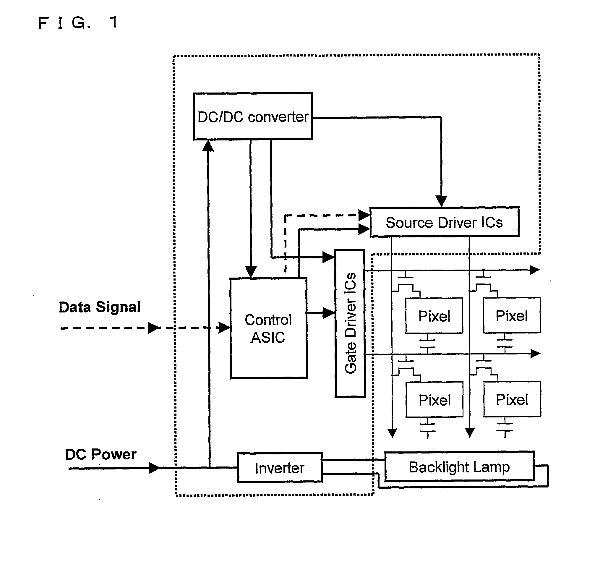
[0091]In a preferred embodiment, the display consists of a standard LCD display, with modified control electronics. An LCD display generally consists of several component parts including:

[0092]1. A backlighting unit to supply even, wide angle illumination to the panel.

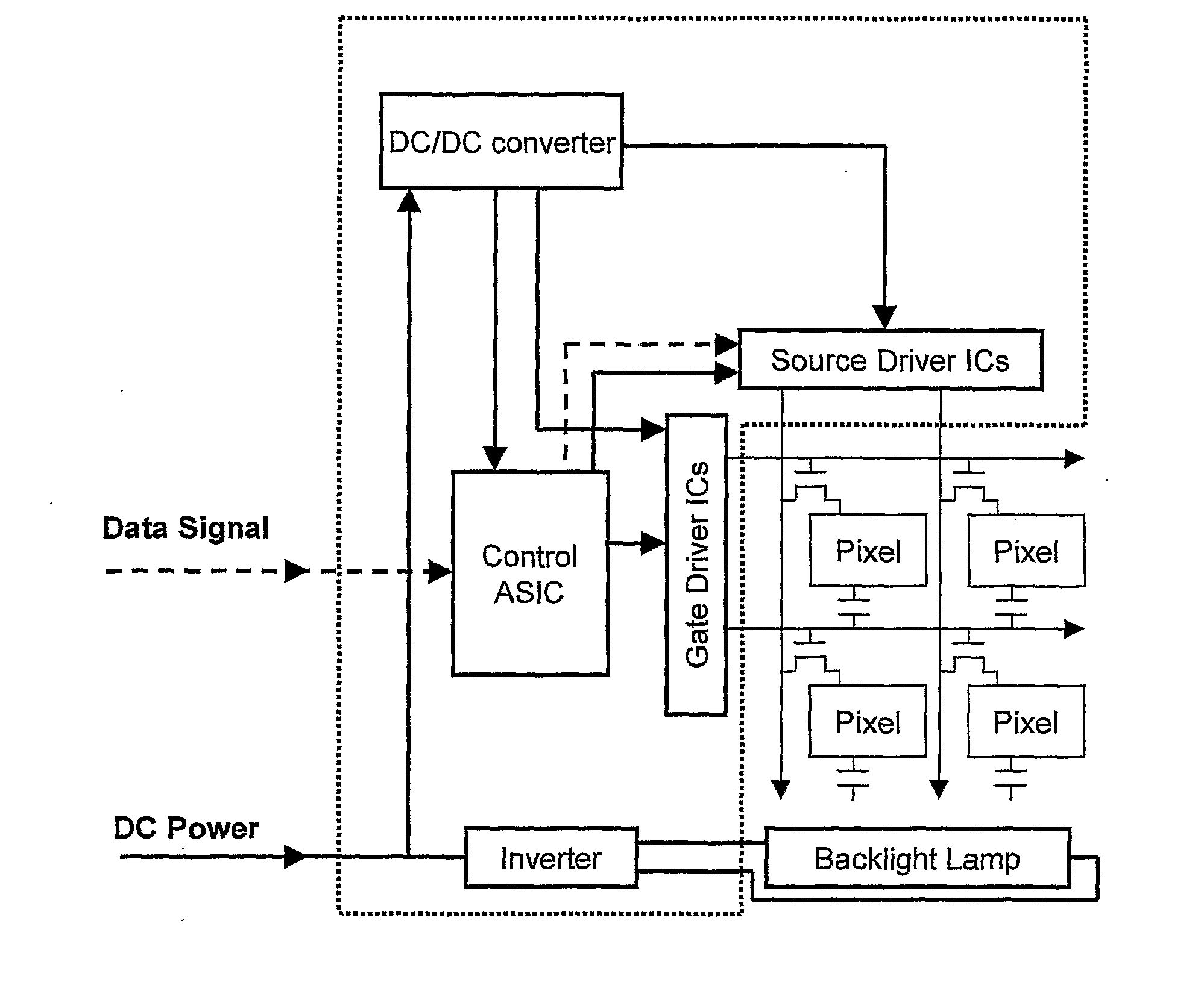
[0093]2. Control electronics to receive digital image data and output analogue signal voltages for each pixel, as well as timing pulses and a common voltage for the counter electrode of all pixels. A schematic of the standard layout of an LCD control electronics is shown in FIG. 1 (Ernst Lueder, Liquid Crystal Displays, Wiley and sons Ltd, 2001).

[0094]3. An LC panel, for displaying an image by spatial light modulation, consisting of a two opposing glass substrates, onto one of which is disposed an array of pixel electrodes and active matrix array to direct the electronic signals, received from the control electronics, to the pixel electrodes. Onto the other substrate is usually disposed a uniform common electrode and c...


PUM


Abstract

A display device is provided that comprises a liquid crystal display panel (2) for displaying an image by spatial light modulation. The image is represented by a plurality of image elements each having an image data value (7). The display device further comprises a display controller (1) arranged to determine a signal voltage to be applied to the panel (2) for each image element in dependence upon its image data value (7) and a secondary data value (8) for the element, there being a predetermined mapping between the data values and the signal voltage. The secondary data values (8) are arranged to vary across the image so as to introduce variations in luminance as a result of the mapping. The mapping and secondary data values (8) are mutually arranged to take account of the signal voltage to on-axis luminance response of the panel (2) so that the luminance variations introduced on-axis tend to balance locally through spatial averaging to, and hence would not be perceivable by, an on-axis viewer (3). The panel (2) furthermore has a non-linear off-axis luminance to on-axis luminance relationship, so that at least some of the luminance variations introduced off-axis do not balance locally through spatial averaging to, and hence would be perceivable by, an off-axis viewer (4).

Description

TECHNICAL FIELD[0001]The present invention relates to a display device, such as an active matrix liquid crystal display device, which is switchable between a public and private display mode.BACKGROUND ART[0002]In a first, public, mode of a display device that is switchable between a public and private display mode, the device commonly behaves as a standard display. A single image is displayed by the device to as wide a viewing angle range as possible, with optimum brightness, image contrast and resolution for all viewers. In the second, private mode, the main image is discernible only from within a reduced range of viewing angles, usually centred on the normal to the display surface. Viewers regarding the display from outside this reduced angular range will perceive either a second, masking image which obscures the main image, or a main image so degraded as to render it unintelligible.[0003]This concept can be applied to many devices where a user may benefit from the option of a pri...

Claims


Application Information

Patent Timeline
Patent Type & Authority Applications(United States)
IPC IPC(8): G09G5/10G09G3/28
CPCG02F1/1323G09G3/003G09G2320/068G09G2320/028G09G2320/0285G09G3/3648G09G3/36
Inventor BROUGHTON, BENJAMIN JOHNEVANS, ALLENGASS, PAUL ANTONYJONES, GRAHAM ROGERKAY, ANDREWWALTON, HARRY GARTHYASUMOTO, TAKASHIINAMORI, YOSHIMITSUMAEDA, KENJI
Owner SHARP KK
Learn More