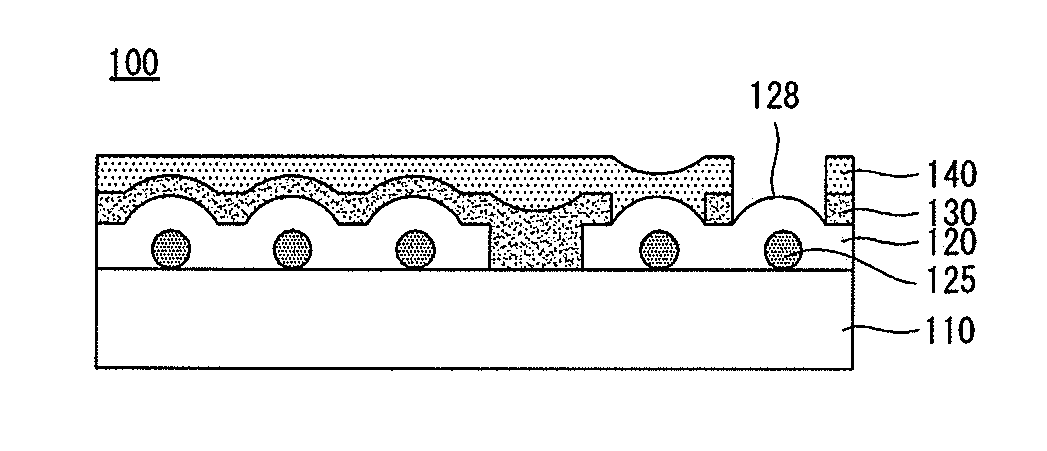
Thin film solar cell and manufacturing method for the same
a solar cell and film technology, applied in the field of thin film solar cells, can solve the problems of shortening the tact time of the process, affecting the production efficiency of solar cells, and not widely used commercial solar cells utilizing single crystal bulk silicon, so as to reduce the manufacturing time, prevent degradation of electrical characteristics of solar cells, and easily form unfavorable first electrodes.
- Summary
- Abstract
- Description
- Claims
- Application Information
AI Technical Summary
Benefits of technology
Problems solved by technology
Method used
Image

Examples
embodiment 1
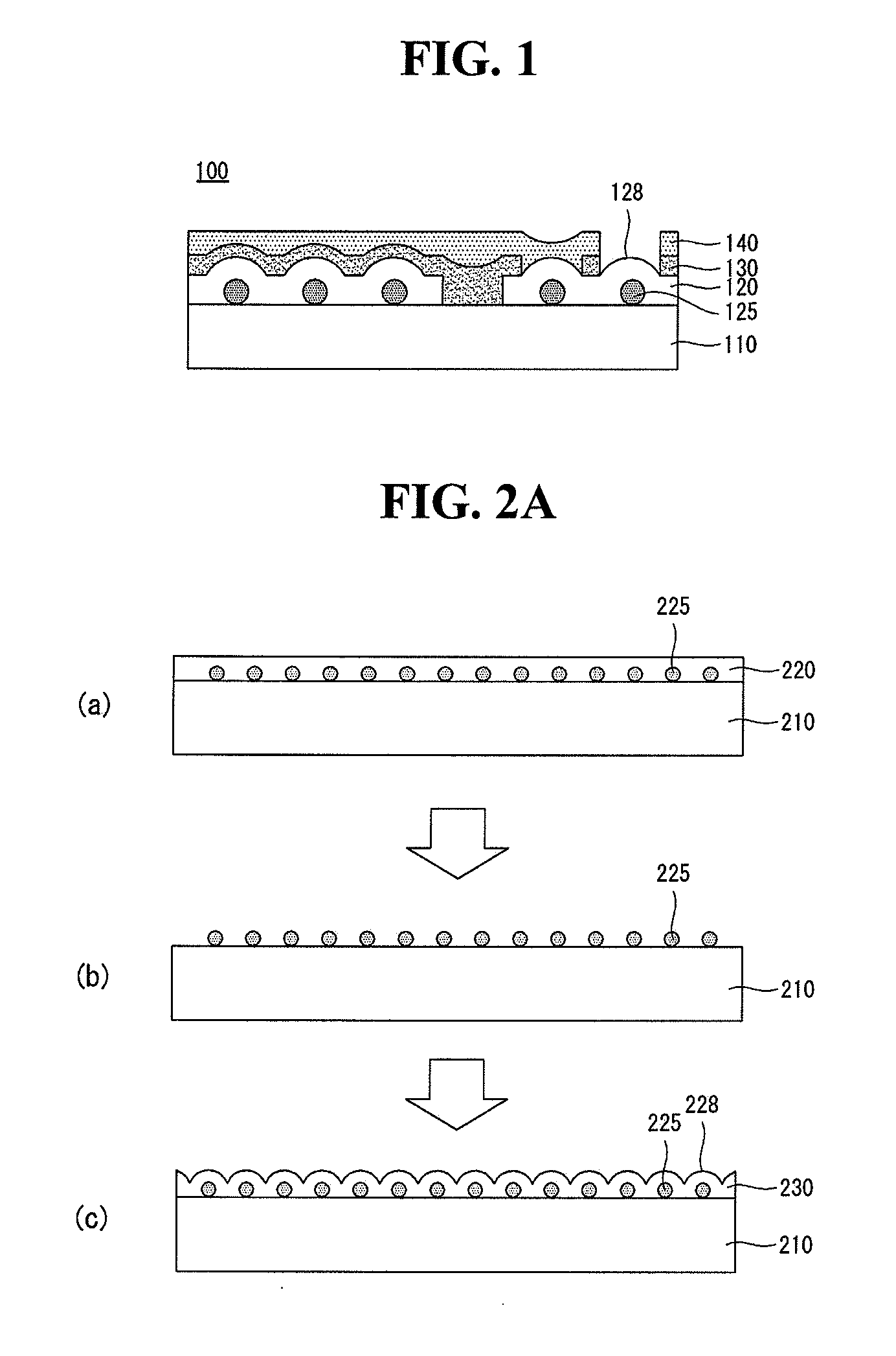
[0085]A glass substrate is coated with solution where gallium-doped zinc oxide (ZnO) particles with a size of 0.7 μm are dissolved. The glass substrate undergoes heating process for five minutes in an oven at 150° C., by which the solution is removed. Subsequently, a first electrode is formed by depositing zinc oxide (ZnO) on the glass substrate with a thickness of 0.4 μm by using a sputtering method.
embodiment 2
[0086]A glass substrate is coated with solution where gallium-doped zinc oxide (ZnO) particles with a size of 0.4 μm are dissolved. The glass substrate undergoes heating process for five minutes in an oven at 150° C., by which the solution is removed. Subsequently, a first electrode is formed by depositing zinc oxide (ZnO) on the glass substrate with a thickness of 0.4 μm by using a sputtering method.
[0087]Table 1 shows measured sheet resistance and transmittance of a first electrode manufactured according to the first and second embodiment. The surface of the first electrode has been measured by SEM; FIGS. 3A and 3B illustrate the measurement result.
TABLE 1Sheet resistance (Ω / sq)Transmission (%)Embodiment 13593Embodiment 23091
[0088]According to the Table 1 and FIGS. 3A and 3B, it can be noticed that both the sheet resistance and transmittance of a first electrode manufactured according to the first and second embodiment satisfy the criteria for mass production.
[0089]As described ab...
PUM
 Abstract
Description
Claims
Application Information
 - R&D
- Intellectual Property
- Life Sciences
- Materials
- Tech Scout
- Unparalleled Data Quality
- Higher Quality Content
- 60% Fewer Hallucinations
Browse by: Latest US Patents, China's latest patents, Technical Efficacy Thesaurus, Application Domain, Technology Topic, Popular Technical Reports.
© 2025 PatSnap. All rights reserved.Legal|Privacy policy|Modern Slavery Act Transparency Statement|Sitemap|About US| Contact US: help@patsnap.com