
Optical waveguide substrate and substrate mounting photoelectric hybrid circuit

a photoelectric hybrid circuit and optical waveguide technology, applied in the direction of optical waveguide light guide, instruments, optics, etc., can solve the problems of increasing the number of lines or measures against cross talk in the conventional electrical line, and achieve the effects of saving costs, reducing parts and fabrication steps, and high-density wiring

Inactive Publication Date: 2010-07-01
HITACHI CHEM CO LTD
View PDF4 Cites 12 Cited by
  • Summary
  • Abstract
  • Description
  • Claims
  • Application Information

AI Technical Summary

Benefits of technology

[0014]According to the present invention, there may be provided a substrate mounting a photoelectric hybrid circuit that has an optical path conversion mirror structure and optical waveguide wiring that may reduce the number of parts and the number of fabrication steps to save the costs, as well as most effectively implement high-density wiring in an optical connection between the optical waveguide and the photoelectric conversion element or optical waveguide array connector that are formed on the substrate, and a device using the substrate mounting the photoelectric hybrid circuit.

Problems solved by technology

As the system is developed to process huge amount of information, for example, of more than several terabits / sec, problems with the number of lines or measures against cross talk become more serious in the conventional electrical lines.

Method used


Image

  • Optical waveguide substrate and substrate mounting photoelectric hybrid circuit
  • Optical waveguide substrate and substrate mounting photoelectric hybrid circuit
  • Optical waveguide substrate and substrate mounting photoelectric hybrid circuit

Examples


first embodiment

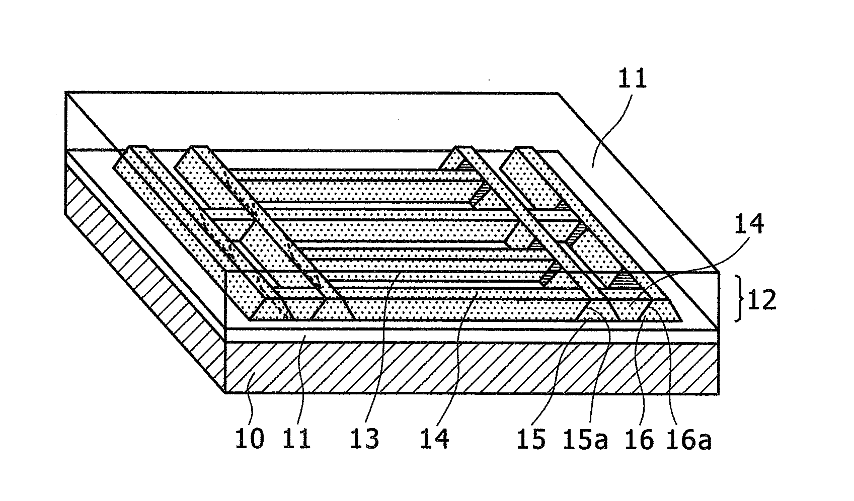
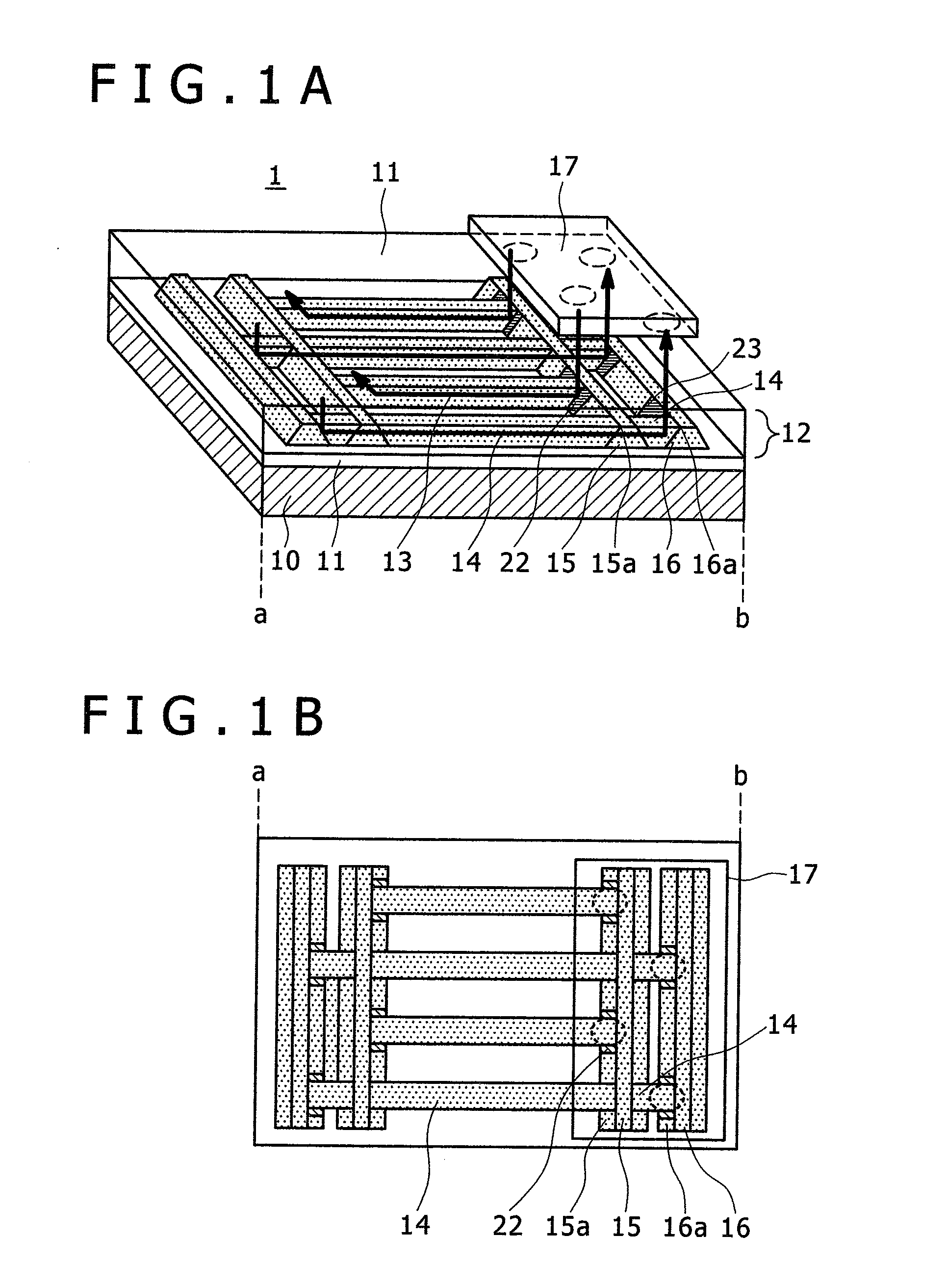
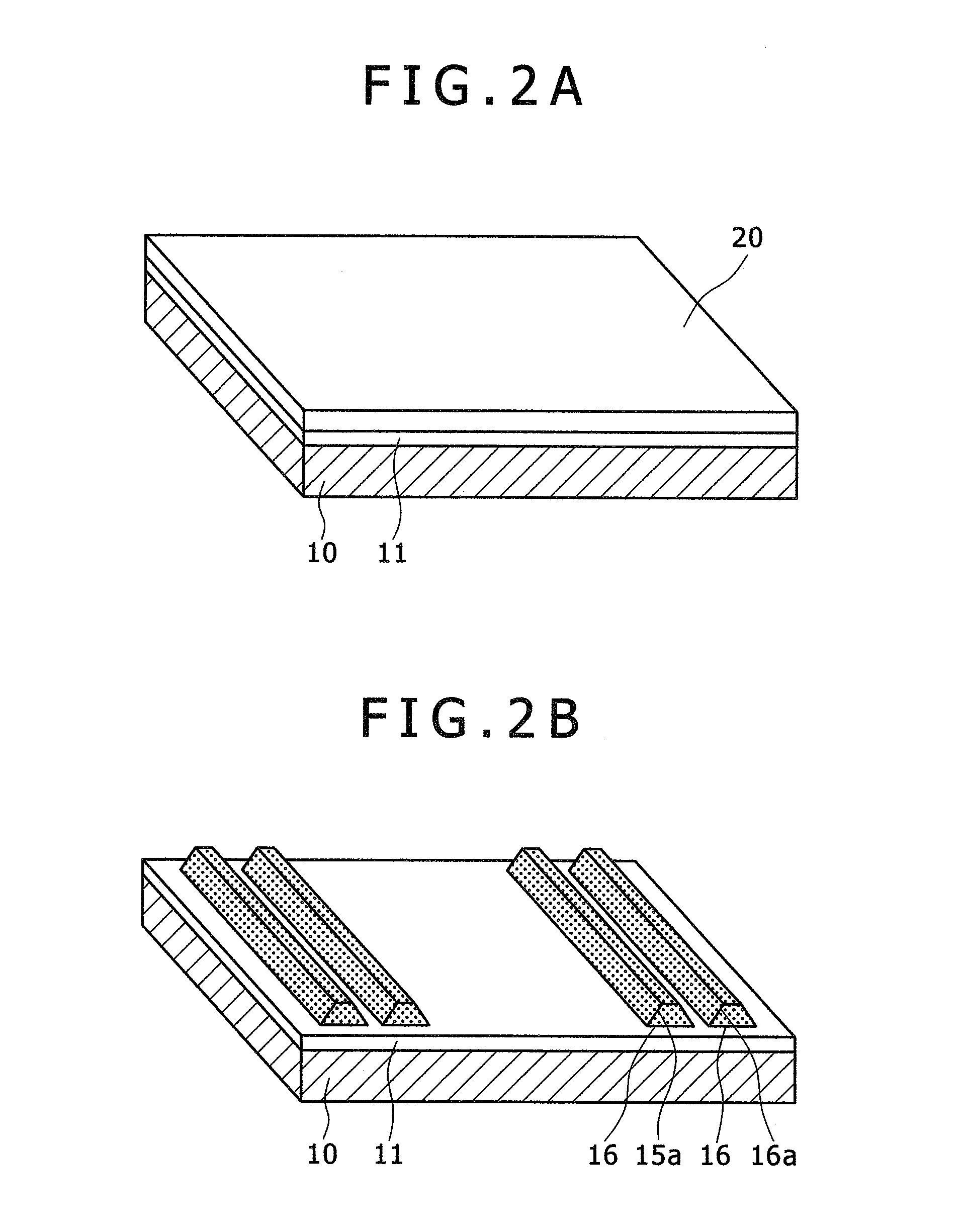
[0016]FIGS. 1A and 1B are a perspective view and a plan view respectively illustrating a photoelectric hybrid circuit-mounted substrate 1 according to a first embodiment of the present invention. Reference numeral 10 refers to a substrate made of a material such as glass epoxy, ceramic, or semiconductor. An optical waveguide layer 12 and cores 15 and 16 are stacked on the substrate 10. The optical waveguide layer 12 has a plurality of wiring cores 13 and 14 therein, each of which is surrounded by a clad layer 11 and made of a material with a high refractive index. Cores 15 and 16 have tapered surfaces 15a and 16a, respectively, which intersect the wiring cores 13 and 14 on the substrate.

[0017]Optical reflecting films 22 and 23 are provided anywhere on the tapered surfaces 15a and 16a of the cores 15 and 16 with tapered surfaces, respectively. Further, the tapered surfaces 15a and 16a are buried in the intersecting wiring cores 13 and 14, respectively. That is, the first wiring core ...

second embodiment

[0024]FIG. 4A,B is a perspective view and a plan view respectively illustrating a photoelectric hybrid circuit-mounted substrate 2 according to a second embodiment of the present invention. In the example shown in FIG. 4A,B, the structure of the photoelectric hybrid circuit-mounted substrate 1 shown in the first embodiment is stacked in double layers. Referring to FIG. 4A,B, a core 41 whose optical path is turned by a tapered surface 43a of a core 43 with the tapered surface and a core 42 whose optical path passes through the core 43 with the tapered surface and is turned by a tapered surface 44a of a core 44 with the tapered surface are alternately arranged in an optical waveguide layer 40 similarly to the structure of the photoelectric hybrid circuit-mounted substrate 1. The optical waveguide layer 40 is arranged on the optical waveguide layer 12 in the thickness direction. And optical element arrays 17 are positioned on the surface of the optical waveguide layer 40 to correspond ...

third embodiment

[0025]FIG. 5 is a perspective view illustrating a photoelectric hybrid circuit-mounted substrate 3 according to a third embodiment of the present invention. In this embodiment, the cores 15 and 16 with the tapered surfaces included in the optical waveguide layer 12 are arranged immediately under the cores 43 and 44 with the tapered surfaces included in the optical waveguide layer 40 in the two-layer lamination structure of the photoelectric hybrid circuit mounting substrate 2 according to the second embodiment. Referring to FIG. 5, light propagating through the core 14 in the optical waveguide layer 12, which is indicated by dotted lines in FIG. 5, turns its optical path upwardly from the substrate by the tapered surface 15a of the core 15 with the tapered surface, passes through the core 43 with the tapered surface included in the optical waveguide layer 40, and then turns the optical path in parallel with the substrate by the tapered surface 43a. The light whose optical path has b...


PUM


Abstract

There are provided a substrate mounted with a photoelectric hybrid circuit having an optical path conversion mirror structure and optical waveguide wiring by reducing the number of parts and the number of fabrication steps, as well as most effectively implement high-density wiring for an optical connection between the optical waveguide and the photoelectric conversion element or optical waveguide array connector that are formed on the substrate, and a device. An optical waveguide layer 12 stacked on a substrate 10 and formed of a wiring core surrounded by a clad layer 11, and cores 15, 16 having tapered surfaces intersecting the respective wiring cores 13, 14 of the optical waveguide layer 12 perpendicularly are arranged, the tapered surfaces 15a, 16a of the cores 15, 16 having tapered surfaces are buried respectively in the wiring portion cores intersecting perpendicularly, and a first core 13 for turning the optical path of light propagating through the wiring portion core at the first core 15 with a tapered surface, and a second core 14 for turning the optical path of light passed through the first core 15 with a tapered surface at the second core 16 with a tapered surface are arranged alternately.

Description

TECHNICAL FIELD[0001]The present invention relates to an optical waveguide substrate and a substrate mounting a photoelectric hybrid circuit, and particularly to a method of mounting an optical wiring structure and an optical connection unit that are included in a photoelectric hybrid circuit mounting substrate, which batch process huge amounts of optical signals transmitted and received between boards in a transmission device.BACKGROUND ART[0002]In recent years, communication traffic upgrade has been swiftly made to exchange huge amounts of data at high speed by using light in the information communication area. Currently, long-haul fiber optic networks, such as backbone, metro, and access networks, spread over a relatively long distance that reaches a few kilometers or more. Further, existing signal lines are being replaced with fiber-optic lines in order to process huge amount of data without delay even for a very short distance between transmission devices (several meters to sev...

Claims


Application Information

Patent Timeline
Patent Type & Authority Applications(United States)
IPC IPC(8): G02B6/12
CPCG02B6/12002G02B6/4214G02B6/43G02B6/122G02B6/42
Inventor MATSUOKA, YASUNOBUSHISHIKURA, MASATO
Owner HITACHI CHEM CO LTD
Learn More