
Light emitting device

a technology light source, which is applied in the direction of waveguides, lighting and heating apparatus, instruments, etc., can solve the problems of poor solder connection, excessive thermal resistance of light emitting device in this configuration, and poor light output of light emitting device, so as to reduce the reduction of light output, improve light output, and efficiently direct light outward

Active Publication Date: 2010-07-01
MATSUSHITA ELECTRIC WORKS LTD
View PDF3 Cites 35 Cited by
  • Summary
  • Abstract
  • Description
  • Claims
  • Application Information

AI Technical Summary

Benefits of technology

[0013]A light emitting device in the present invention has been accomplished in view of the above problem, and intended to suppress an improper solder connection at electrodes and to precisely position an optical member.
[0015]The light emitting device in the present invention enables to prevent void-generation in the encapsulation resin, as well as allowing to precisely position the optical member. In this configuration, an inner circumference of the ring gate is spaced from the optical member. This configuration enables to prevent an extra encapsulation resin from flowing to the electrodes, thereby being free from improper solder connection at the electrodes. Compared to a conventional light emitting device in which the mounting substrate is provided with a recess receiving the LED chip and a portion of the optical member, the light emitting device in the present invention enables to suppress the reduction of light output resulting from light absorption in the mounting substrate, for efficiently directing light outward to give an improved light output.
[0016]In this invention, the color conversion member is preferably formed at inner peripheral bottom rim with a recess which engages with the ring gate, for being more precisely positioned. In this configuration, it is possible to shorten an interval between the color conversion member and the optical member.
[0017]More preferably, the ring gate is formed of a white resist in the present invention. The ring gate is prevented from absorbing the light which is emitted from the LED chip and the phosphor, enabling to achieve a high light output.
[0018]More preferably, the mounting substrate includes a heat conducting plate made of a heat conductive material and a printed substrate having an opening. A sub-mount member mounting the LED chip thereon is disposed directly on a top surface of the heat conducting plate to pass through the opening of the printed substrate. The opening of the mounting substrate is filled with the encapsulation resin around a periphery of the sub-mount member. The sub-mount member is configured to relieve a stress acting on the LED chip due to a difference of coefficient of linear expansion between the LED chip and the heat conducting plate, as well as thermally coupling the LED chip to the heat conducting plate. This configuration enables to prevent the LED chip from being broken due to the difference of coefficient of linear expansion between the LED chip and the heat conducting plate, thereby giving a highly reliable light emitting device. In this configuration, the sub-mount member is designed to be thick enough to prevent the light emitted from the LED chip, from being absorbed in the printed substrate, so as to achieve a high light output.

Problems solved by technology

But, the light emitting device in this configuration may suffer from an excessive thermal resistance between a light emitting part of the LED chip 110 and main body.
Namely, this light emitting device may not give a high light output.
However, in the process of disposing the color conversion member 170 securely to the mounting substrate 120 in this configuration, an extra encapsulation resin overflowing from the groove 129 may flow to electrodes which are exposed outside of the color conversion member 170, eventually causing a poor solder connection.
This light emitting device may suffer from void-generation inside the encapsulation resin 150, possibly giving a lowered light output.

Method used


Image

  • Light emitting device
  • Light emitting device
  • Light emitting device

Examples


Embodiment Construction

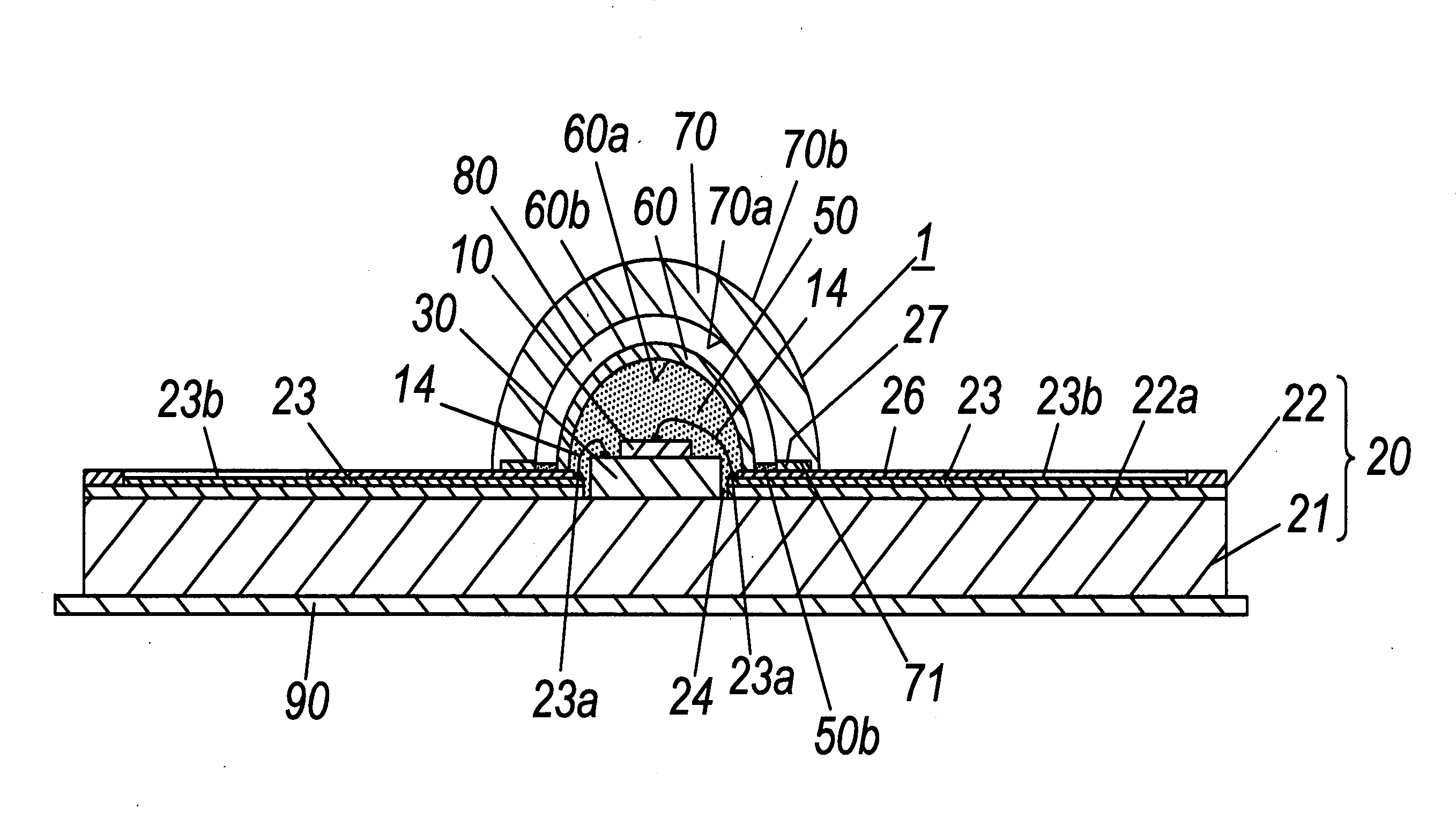
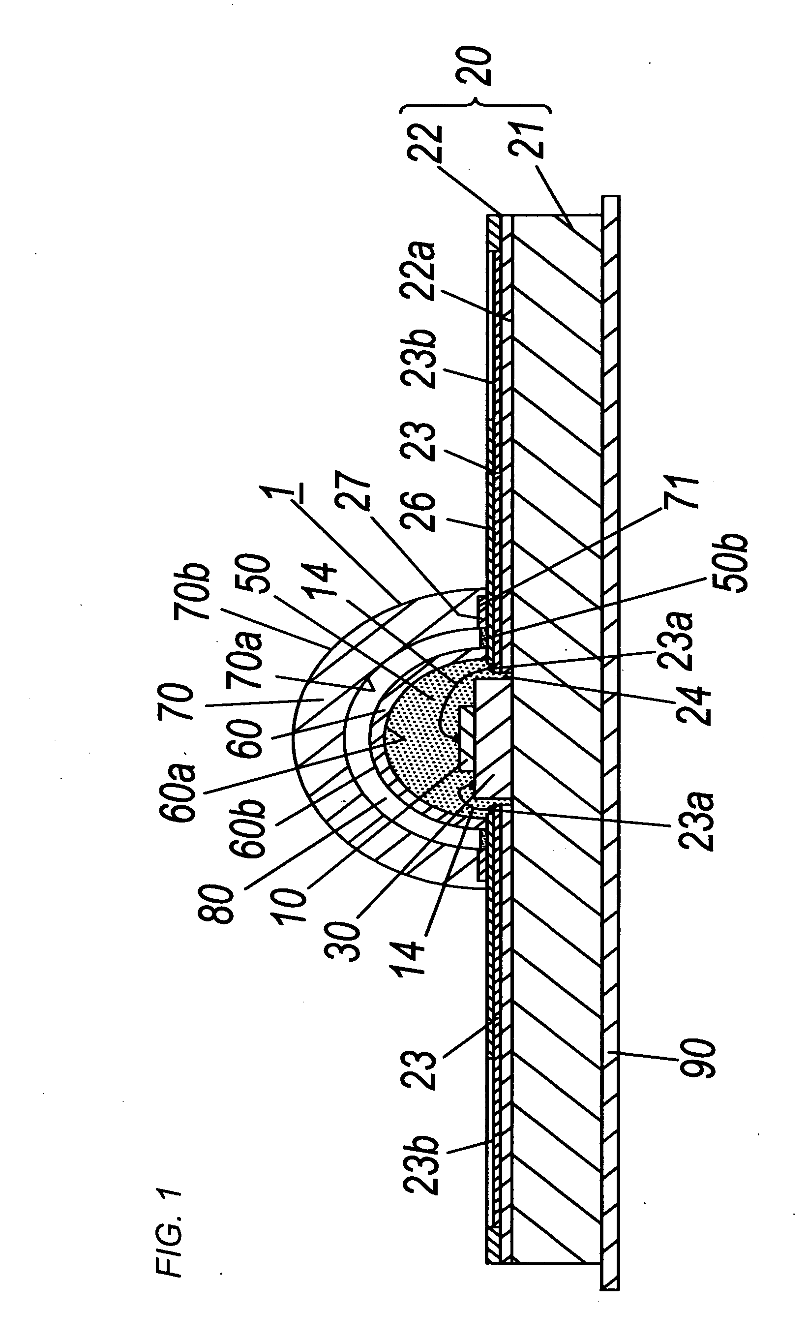
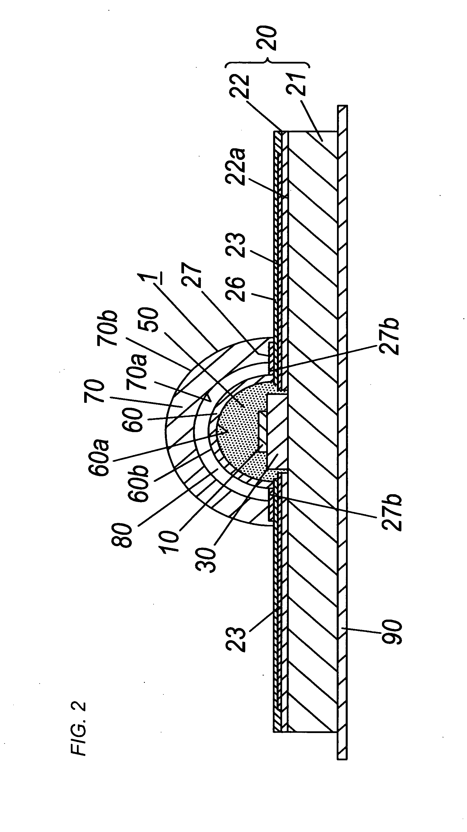
[0033]Hereafter, explanations are given as to a light emitting device in this embodiment, with reference to FIGS. 1 to 7.

[0034]The light emitting device 1 in this embodiment comprises an LED chip 10, a mounting substrate 20 shaped into a rectangular plate which holds the LED chip 10, a dome-shaped optical member 60 made of a light-transmissive material, a light-transmissive elastic encapsulation resin 50, and a dome-shaped color conversion member 70. The mounting substrate 20 is provided at its top surface with a ring gate 27. The ring gate 27 is formed outside of the optical member 60 to protrude from the top surface of the mounting substrate. The mounting substrate 20 is provided at its top surface with the LED chip 10 and a patterned conductor 23 which supplies electric power to the LED chip 10. The encapsulation resin 50 is filled in a space confined between the optical member 60 and the mounting substrate 20 for encapsulating therewith the LED chip 10 and a plurality of (two in...


PUM


Abstract

A light emitting device, in which an encapsulation resin is disposed at a space confined between an optical member and a mounting substrate. This encapsulation resin is possibly made free from a void-generation therein. In this light emitting device, the optical member can be precisely positioned. An electrode disposed outside a color conversion member is possibly free from an improper solder connection. A ring gate is formed on the top surface of the mounting substrate outside of the optical member, and acts to position the color conversion member. The ring gate acts to prevent an overflowing liquid encapsulation resin from flowing to the electrode provided. The ring gate is provided with a plurality of centering projections which are spaced circumferentially along its inner circumference to position the color conversion member.

Description

TECHNICAL FIELD[0001]This invention relates to a light emitting device using LED chip (light emitting diode chip).BACKGROUND ART[0002]Many studies have been widely carried out to develop light emitting device so far. The light emitting device includes an LED chip and a phosphor. (e.g., Reference 1) The phosphor is employed as a wavelength conversion member which is excited by a light emitted from LED chip and radiates a light of color different from the luminescent color of the LED. The light emitting device is capable of radiating a light of mixed-color which is different from the luminescent color of LED, when including the phosphor and the LED chip. For example, the light emitting device is commercially available as a white-colored light emitting device (generally referred to as a white-color LED), in which the LED chip emitting blue-color or UV light is combined with the phosphor to give white-color light (white-color luminescent spectrum).[0003]The reference 1 discloses one exa...

Claims


Application Information

Patent Timeline
Patent Type & Authority Applications(United States)
IPC IPC(8): H01L33/00H01L33/32H01L33/50H01L33/56H01L33/62
CPCH01L33/486H01L33/507H01L33/52H01L33/58H01L2224/48091H01L2924/00014H01L2224/45124H01L2224/45144Y10S385/901H01L2924/00F21K9/00H01L33/505H01L33/62H01L33/64H05K1/141H05K1/184H05K3/0061H05K2201/0311H05K2201/048H05K2201/10106H05K2201/10121H05K2201/10962F21Y2105/10F21Y2115/10
Inventor URANO, YOUJI
Owner MATSUSHITA ELECTRIC WORKS LTD
Learn More