Semiconductor device and manufacturing method thereof

a technology of semiconductor devices and semiconductor films, applied in semiconductor devices, capacitors, electrical devices, etc., can solve the problems of reducing the penetration velocity of hydrofluoric acid to the interlayer insulating film under the support film, affecting the function of supporting the lower electrode, and affecting the stability of the lower electrode, etc., to achieve the effect of large capacity, convenient manufacturing and superior data storage characteristics

Active Publication Date: 2010-06-17
LONGITUDE LICENSING LTD
View PDF9 Cites 33 Cited by
  • Summary
  • Abstract
  • Description
  • Claims
  • Application Information

AI Technical Summary

Benefits of technology

[0025]For a semiconductor device such as a DRAM having a 6F2 memory cell, collapsing of lower electrodes of capacitors during a manufacturing process can now be prevented and lower electrodes with tall heights can be readily manufactured. Therefore, even with developments in miniaturization, a memory cell of a DRAM having large-capacitance capacitor elements can be manufactured and a semiconductor device such as a DRAM featuring a large capacity and superior data storage characteristics (refresh characteristics) can be readily manufactured.

Problems solved by technology

However, the present inventor has discovered that providing capacitor lower electrodes arranged in a closest-packing arrangement with a support film for preventing collapsing has the following problems.
Firstly, in a wet etching process for exposing the side surfaces of the lower electrodes of capacitors, the penetration velocity of a chemical (hydrofluoric acid) to an interlayer insulating film under the support film is reduced. Consequently, the support film itself ends up being exposed to the chemical over a longer period of time. Therefore, in wet etching using hydrofluoric acid, since etching of silicon nitride that makes up the support film also proceeds gradually, the extended exposure to the chemical problematically damages the support film and impairs the function of supporting the lower electrodes.
Secondly, with the generation of miniaturized elements based on a design rule of 70 nm or less, there is a problem in that it is difficult to accurately form a pattern of openings 105 with minute sizes even with a state-of-the-art exposure apparatus.
However, when attempting to arrange a large number of lower electrodes with high aspect ratios in the arrangement method illustrated in FIG. 17, an extended length in the X-direction of the support film fixed at both ends thereof caused new problems including curving (displacement) of the support film in the Y-direction as seen in the diagram and an occurrence of partial cracks 111 in the support film itself.
Therefore, collapsing of the lower electrodes could not be prevented.

Method used


Image

  • Semiconductor device and manufacturing method thereof
  • Semiconductor device and manufacturing method thereof
  • Semiconductor device and manufacturing method thereof

Examples


Embodiment Construction

[0036]The invention will be now described herein with reference to illustrative embodiments. Those skilled in the art will recognize that many alternative embodiments can be accomplished using the teachings of the present invention and that the invention is not limited to the embodiments illustrated for explanatory purposes.

[0037]Preferred embodiments of the present invention will now be described with reference to the drawings.

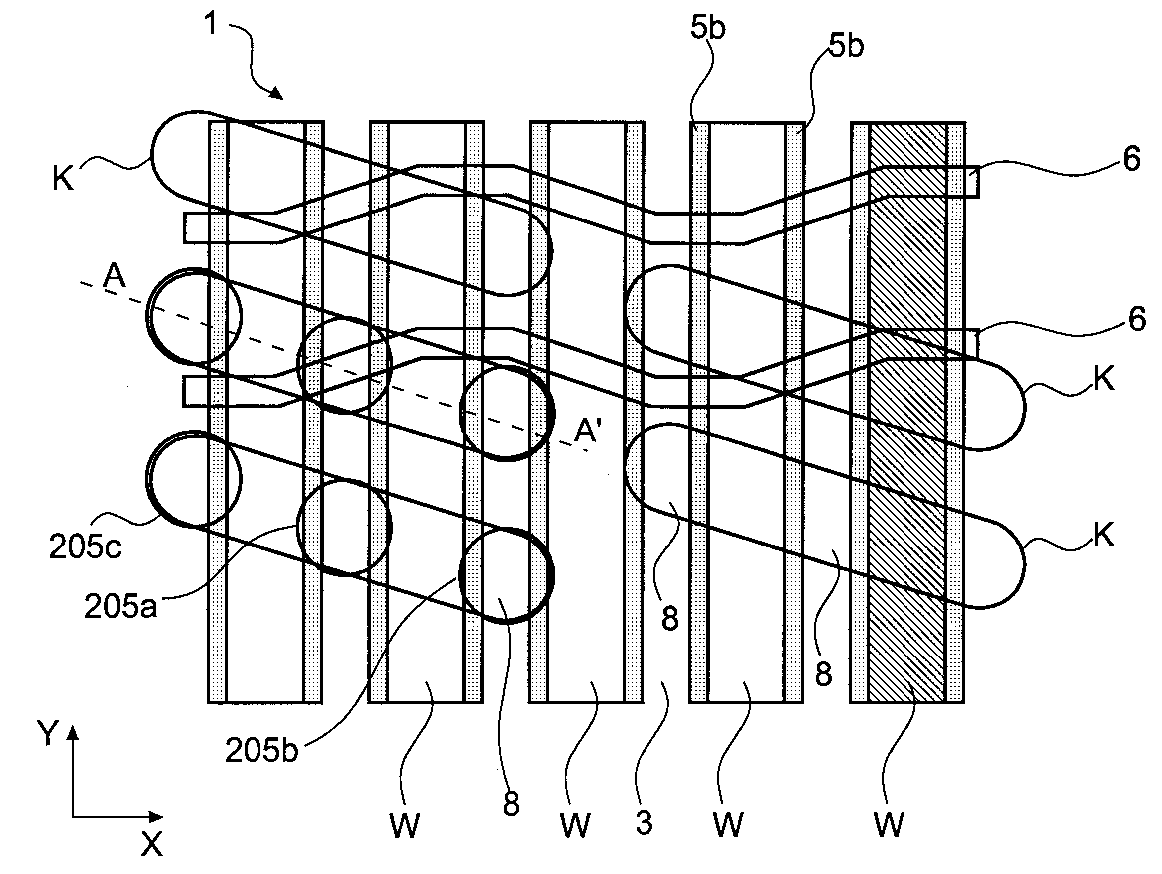
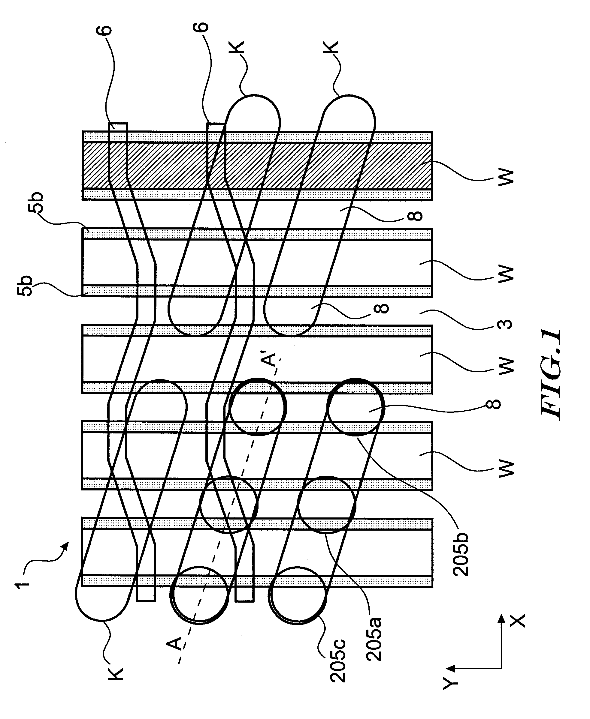
[0038]FIG. 1 is a conceptual diagram illustrating a planar structure of a memory cell part of a DRAM of a semiconductor device according to an embodiment of the present invention, and illustrates only partial components including a memory cell.

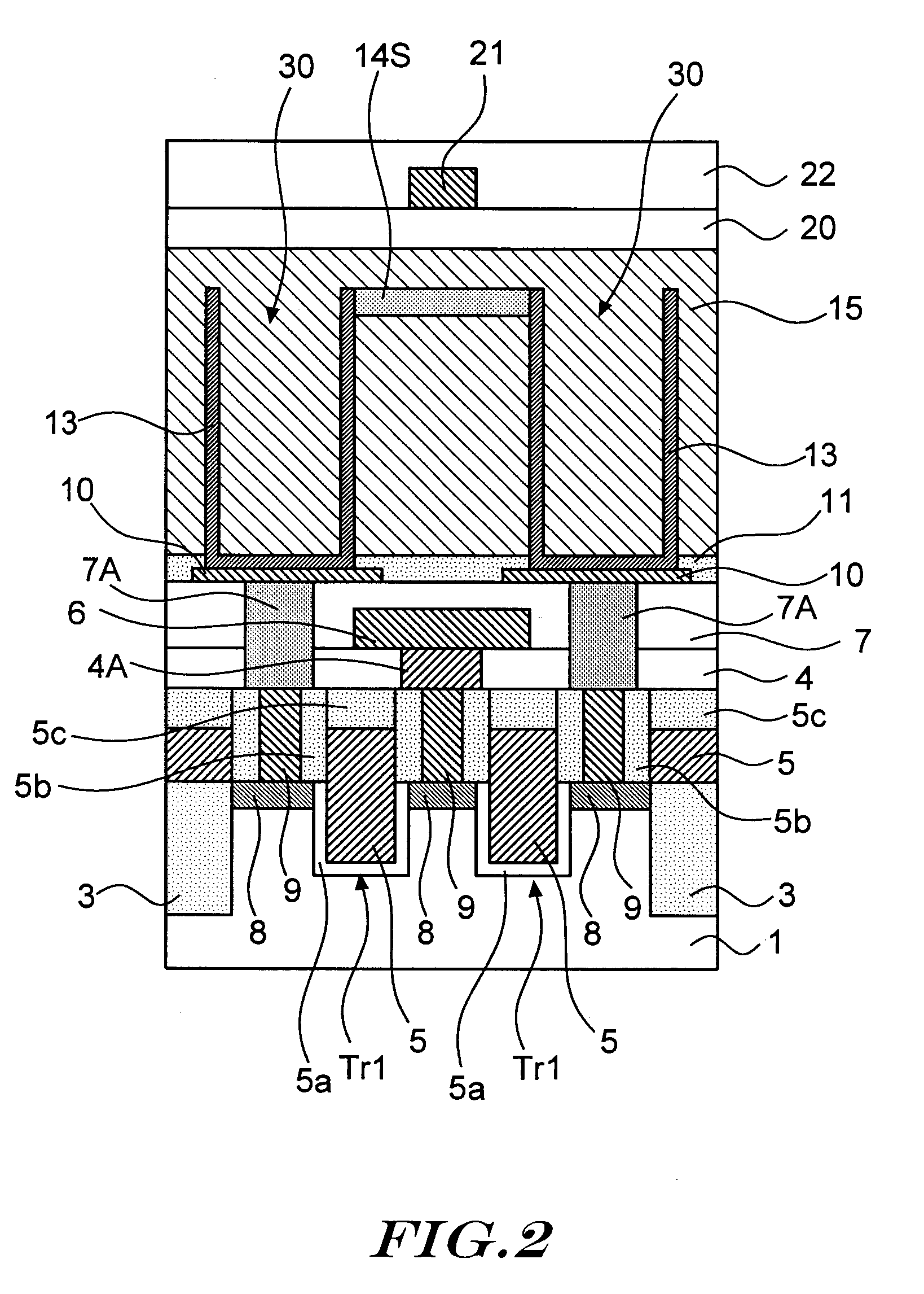
[0039]FIG. 2 is a schematic cross-sectional diagram corresponding to line A-A′ in FIG. 1. The diagrams merely describe a configuration of a semiconductor device and the sizes, dimensions and the like of the respective illustrated parts may differ from the dimensional relationships of an actual semiconductor device.

[0040...


PUM


Abstract

A semiconductor device having a 6F2 memory cell whose size is defined by a numerical value of a design rule F, wherein: lower electrodes of capacitors included in the memory cell are supported by a support film; the support film is formed as a pattern combining a first support pattern (14x) linearly extending in a first direction and a second support pattern (14y) linearly extending in a second direction that crosses to the first direction; the support film is arranged such that the intervals of the first and second support patterns are both equal to or greater than 1.5F; and the interval of one of the first and second support patterns is greater than the interval of the other one of the first and second support patterns.

Description

BACKGROUND OF THE INVENTION[0001]1. Field of the Invention[0002]The present invention relates to a semiconductor device such as a DRAM (dynamic random access memory) element including a 6F2 memory cell whose size is defined by a numerical value of a design rule F. More specifically, the present invention relates to a semiconductor device including a memory cell part having a supporting part for preventing lower electrodes of capacitors of a memory cell part from collapsing and coming into contact with each other.[0003]2. Description of the Related Art[0004]Developments in miniaturization of semiconductor devices have led to smaller areas of memory cells making up a DRAM. Consequently, it is generally practiced that capacitors making up a memory cell be three-dimensionally formed in order to secure sufficient capacitance at the capacitors. Specifically, by providing a lower electrode of a capacitor with a cylindrical shape and using a sidewall of the lower electrode as a capacitor, s...

Claims


Application Information

Patent Timeline
Patent Type & Authority Applications(United States)
IPC IPC(8): H01L27/108H01L21/20
CPCH01L27/10814H01L28/90H01L27/10852H10B12/315H10B12/033
Inventor KADOYA, TOMOHIRO
Owner LONGITUDE LICENSING LTD
Why Eureka
Try Eureka