Wiring board and method of manufacturing the same

Active Publication Date: 2010-06-17
SHINKO ELECTRIC IND CO LTD
View PDF5 Cites 52 Cited by
  • Summary
  • Abstract
  • Description
  • Claims
  • Application Information

AI Technical Summary

Benefits of technology

[0013]An object of the present invention is to provide a wiring board which allows POP bonding to be easily performed with low costs and enables to achieve an improvement in the reliability of the bonding, and a method of manufacturing the same.
[0015]With the configuration of the wiring board (package) according to this aspect, the second pad is arranged in the electronic component mounting area on the outermost insulating layer, and the first pad arranged in a peripheral region thereof is formed by causing a portion of the insulating layer to protrude in a bump shape, the first pad covering a surface of the portion thereof. Thus, POP bonding can be easily performed. Specifically, when a different package is bonded to the first pad via a solder bump, the gap between the surface of the first pad and an electrode pad of the different package (i.e., the gap between the upper and lower packages) can be made relatively narrow. Thus, without placing an interposer such as used in the conventional art, the upper and lower packages can be easily bonded to each other via a small amount of solder in accordance with the narrowed gap. Consequently, the interposer is no longer needed in performing POP bonding, so that reduction in costs can be achieved.
[0016]Moreover, the gap between the upper and lower packages can be made smaller when POP bonding is performed, so that the amount of usage of solder for bonding the upper and lower packages can be made less as well. As a result, the inconveniences such as separation of solder and formation of a bridge, which are observed in the prior art, can be resolved. This advantage thus contributes to an improvement in the reliability of the bonding between the upper and lower packages.

Problems solved by technology

Accordingly, there arises a problem in that manufacturing costs increase.
Meanwhile, in the case where solder is used for bonding, the gap between the upper and lower packages is large because of the presence of the chip mounted between the packages.
In this case, there are inconveniences such as separation of the bump (separation of the solder) during reflow soldering, and formation of a bridge between adjacent bumps.
This produces a problem in that the reliability of bonding between the upper and lower packages is lowered.

Method used


Image

  • Wiring board and method of manufacturing the same
  • Wiring board and method of manufacturing the same
  • Wiring board and method of manufacturing the same

Examples


first embodiment

See FIGS. 1 to 7

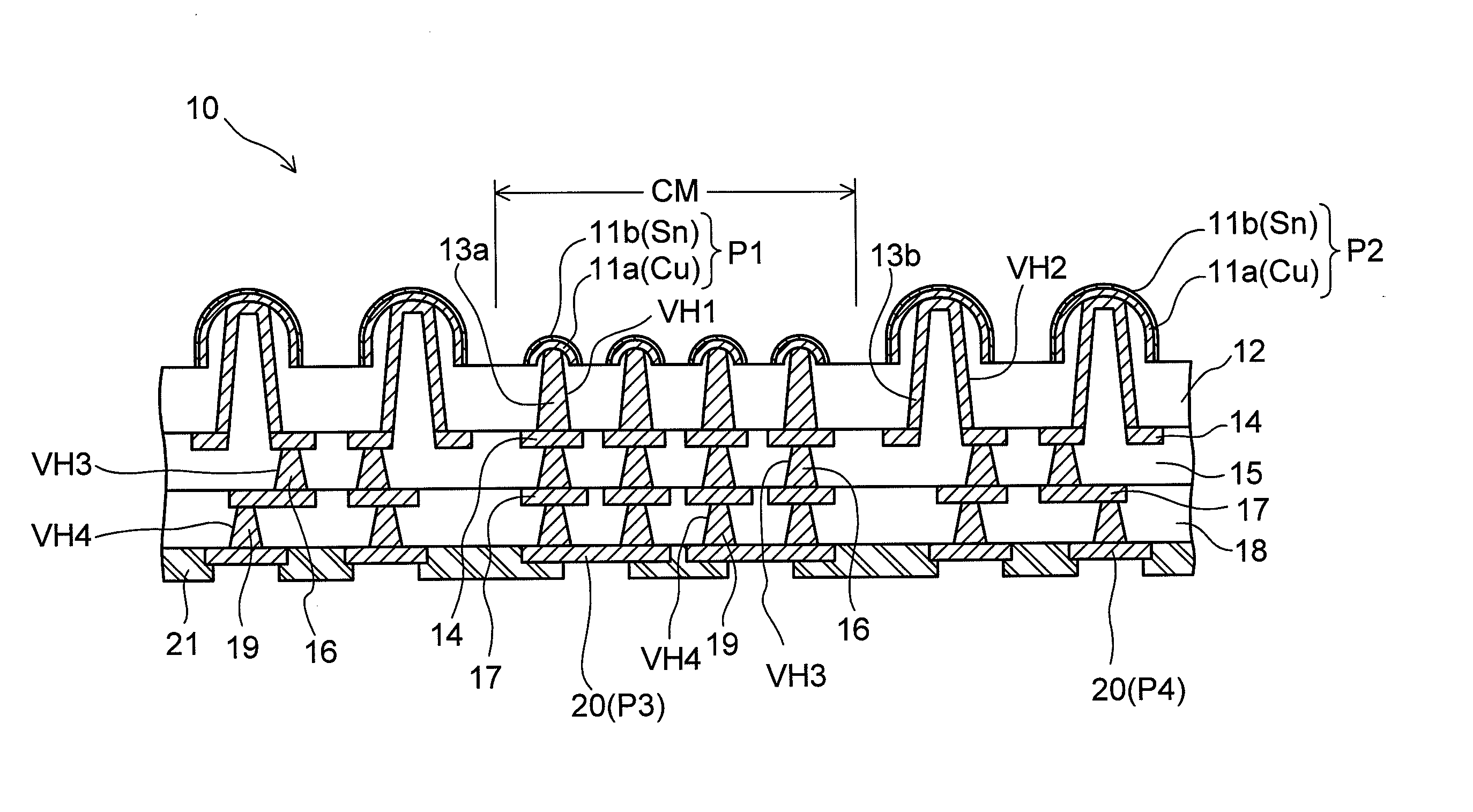
[0032]FIG. 1 shows a configuration of a wiring board (semiconductor package) according to a first embodiment of the present invention, in the form of a cross-sectional view.

[0033]A wiring board (semiconductor package) 10 according to the present embodiment has a structure in which multiple wiring layers 14, 17 and 20 are stacked one on top of another with insulating layers (specifically, resin layers) 12, 15 and 18 interposed between corresponding wiring layers, as illustrated. In this structure, the wiring layers 14, 17 and 20 are connected via conductors (vias 13a and 13b, 16 and 19), respectively, filled into via holes VH1 and VH2, VH3 and VH4 each formed in a corresponding one of the insulating layers 12, 15 and 18. Specifically, the package 10 has the form of a “coreless substrate,” which does not include a support base member, and is different from a wiring board fabricated by using a general build-up process (in which a required number of build up layers are s...

second embodiment

See FIGS. 8 and 9

[0085]FIG. 8 shows a configuration of a wiring board (semiconductor package) according to a second embodiment of the present invention, in the form of a cross-sectional view.

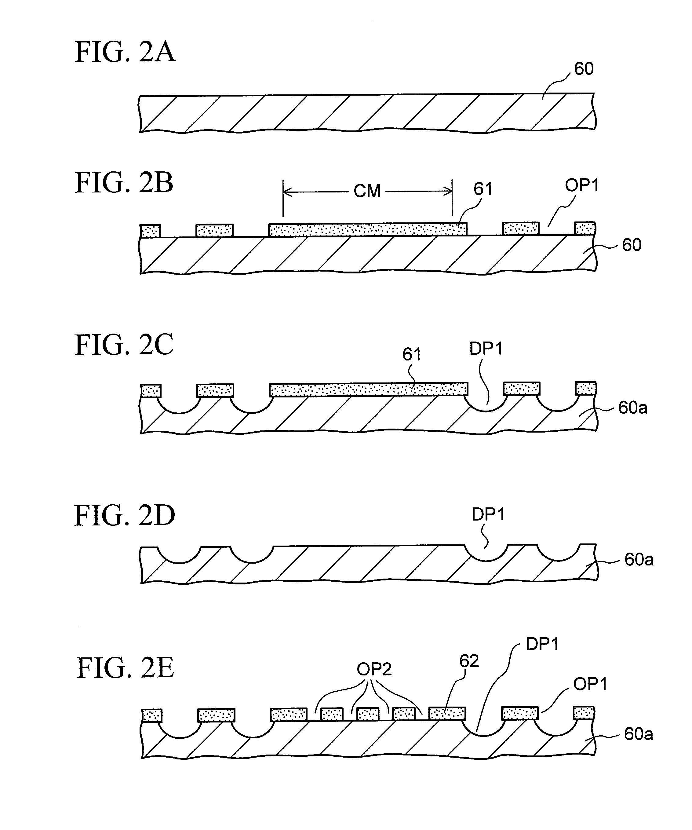
[0086]As compared with the configuration of the wiring board 10 (FIG. 1) according to the first embodiment, a wiring board (semiconductor package) 10a according to the second embodiment is different in the following points. First, the surfaces of pads P5 arranged in the chip mounting area CM are formed at a position recessed from the surface of a resin layer 12a to an inner side of the board by a predetermined depth. Thereby, the recessed portions DP are formed at positions corresponding to the pads P5 on the rein layer 12a, respectively. Second, the pads P5 for mounting a chip and pads P6 for POP bonding arranged in the peripheral region around the pads P5 are both formed of a single metal layer (Cu layer). Since the other configuration of the wiring board 10a is basically the same as the confi...

third embodiment

See FIGS. 10 to 12c

[0096]FIG. 10 shows a configuration of a wiring board (semiconductor package) according to the third embodiment of the present invention, in the form of a cross-sectional view.

[0097]As compared with the configuration of the wiring board 10 (FIG. 1) according to the first embodiment, a wiring board (semiconductor package) 10b according to the third embodiment is different in the following points. First, each of pads P7 arranged in the chip mounting area CM has a structure in which multiple metal layers are stacked one on top of another (for example, a Cu layer, Ni layer and Au layer in the order from the lower layer side), and the surfaces of the pads P7 are exposed and flush with the surface of the resin layer 12b. Second, each of pads P8 for POP bonding arranged in the peripheral region around the chip mounting area CM is formed of a single metal layer (Cu layer). Since the other configuration of the wiring board 10b is basically the same as that of the wiring b...


PUM


Abstract

A wiring board (package) has a structure in which multiple wiring layers are stacked one on top of another with insulating layers each interposed between corresponding two of the wiring layers, and the wiring layers are connected to each other through vias formed in the insulating layers. In the peripheral region around the chip mounting area of the outermost insulating layer on one of both surfaces of the board, a pad is formed in a bump shape to cover a surface of a portion of the outermost insulating layer, the portion being formed to protrude, and a pad whose surface is exposed from the insulating layer is arranged in the chip mounting area. A chip is flip-chip bonded to the pad of the package, and another package is bonded to the bump shaped pad in a peripheral region around the chip (package-on-package bonding).

Description

CROSS-REFERENCE TO RELATED APPLICATIONS[0001]This application is based on and claims priority of Japanese Patent Application No. 2008-321037 filed on Dec. 17, 2008, the entire contents of which are incorporated herein by reference.BACKGROUND OF THE INVENTION[0002](a) Field of the Invention[0003]The present invention relates to a wiring board and a method of manufacturing the same. More specifically, the invention relates to a wiring board having a structure in which terminals (pads) for mounting a semiconductor element (chip) or the like or for external connection are exposed from an outermost insulating layer, and also to a method of manufacturing the same.[0004]The wiring board is also referred to as a “semiconductor package” in the description below, for the sake of convenience, because the wiring board has the role as a package for mounting a semiconductor element (chip) or the like thereon.[0005](b) Description of the Related Art[0006]In a trend to make semiconductor devices sm...

Claims


Application Information

Patent Timeline
IPC IPC(8): H01R12/06H01K3/10H01R12/51
CPCH01L21/4853Y10T29/49162H01L23/49816H01L23/49822H01L23/49838H01L24/16H01L24/17H01L25/105H01L25/50H01L2221/68345H01L2224/13099H01L2224/16H01L2924/01011H01L2924/01029H01L2924/01046H01L2924/01078H01L2924/01079H01L2924/15311H01L2924/1532H01L2924/19041H01L2924/19105H05K1/113H05K3/205H05K3/4007H05K3/4682H05K2201/0367H05K2201/09045H05K2201/09436H05K2201/09527H01L2924/01005H01L2924/01006H01L2924/01033H01L2924/01047H01L25/16H01L2225/1023H01L2225/1058H01L21/4857H01L2224/16238H01L2224/1411H01L2224/16237
Inventor KANEKO, KENTAROATOBE, HIDEMI
Owner SHINKO ELECTRIC IND CO LTD
Why Eureka
Try Eureka