Thin Film Photovoltaic Module With Contoured Deairing Substrate
- Summary
- Abstract
- Description
- Claims
- Application Information
AI Technical Summary
Benefits of technology
Problems solved by technology
Method used
Image
Examples
Embodiment Construction
[0011]Thin film photovoltaic devices of the present invention utilize protective substrates that have a surface that has been modified from a planar state to one having contours formed thereon that serve to direct air away from entrapment points near projecting bus bars of an underlying photovoltaic device.
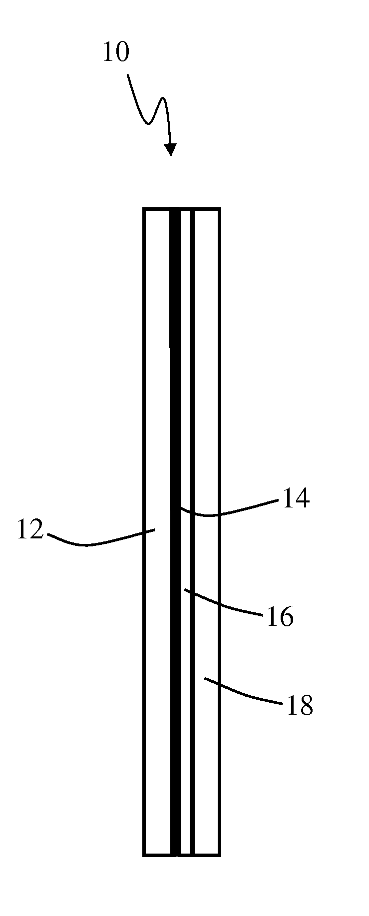
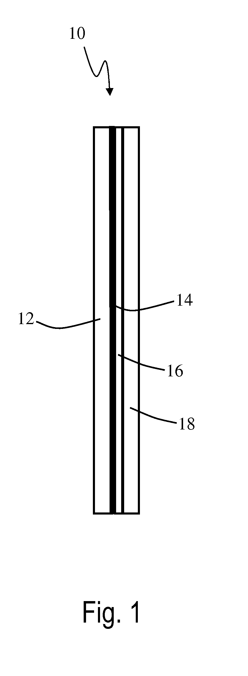
[0012]A schematic representation of the general configuration of a thin film photovoltaic module is shown in FIG. 1 generally at 10. As shown in FIG. 1, a thin film photovoltaic device 14 is formed on a base substrate 12, which can be, for example, glass or plastic. A protective substrate 18 is bound to the photovoltaic device 14 with a polymer layer 16. As described in more detail below, the polymer layer 16 can comprise any suitable polymer.
[0013]Previous attempts to provide a polymer layer that acceptably seals the photovoltaic module have included using polymeric materials that have relatively high flow, using relatively thick sheets of polymer, using higher lamination pressur...
PUM
| Property | Measurement | Unit |
|---|---|---|
| Width | aaaaa | aaaaa |
| Width | aaaaa | aaaaa |
| Depth | aaaaa | aaaaa |
Abstract
Description
Claims
Application Information
 - R&D
- Intellectual Property
- Life Sciences
- Materials
- Tech Scout
- Unparalleled Data Quality
- Higher Quality Content
- 60% Fewer Hallucinations
Browse by: Latest US Patents, China's latest patents, Technical Efficacy Thesaurus, Application Domain, Technology Topic, Popular Technical Reports.
© 2025 PatSnap. All rights reserved.Legal|Privacy policy|Modern Slavery Act Transparency Statement|Sitemap|About US| Contact US: help@patsnap.com


