
System and method for designing multiple clock domain circuits

a design method and clock domain technology, applied in the direction of cad circuit design, program control, instruments, etc., can solve the problems of increasing the complexity of digital circuits, and increasing the limitations of both rtl and behavioral circuit specification techniques, so as to simplify the handling of clocks

Inactive Publication Date: 2010-06-10
BLUESPEC
View PDF19 Cites 9 Cited by
  • Summary
  • Abstract
  • Description
  • Claims
  • Application Information

AI Technical Summary

Benefits of technology

"The present invention provides a HDL tool that simplifies the handling of clocks and signaling between different clock domains in a circuit specification. The tool supports a specific clock data type for use by the designer, which distinguishes clock signals from regular level-sampled signals. The tool also handles clock domain crossing between clock domains driven by clocks of different clock families, either by requiring the use of a synchronizer or by using a linguistic approach to abstract the instantiation of a synchronizer. The technical effects of the invention include improved efficiency and ease of use for designers, as well as improved performance and reliability of the resulting circuits."

Problems solved by technology

Yet as the complexity of digital circuits has increased, both RTL and behavioral circuit specification techniques have shown their limitations.
Furthermore, as with conventional HDLs, HDLs that employ TRS rules typically generate hardware that is synchronous.
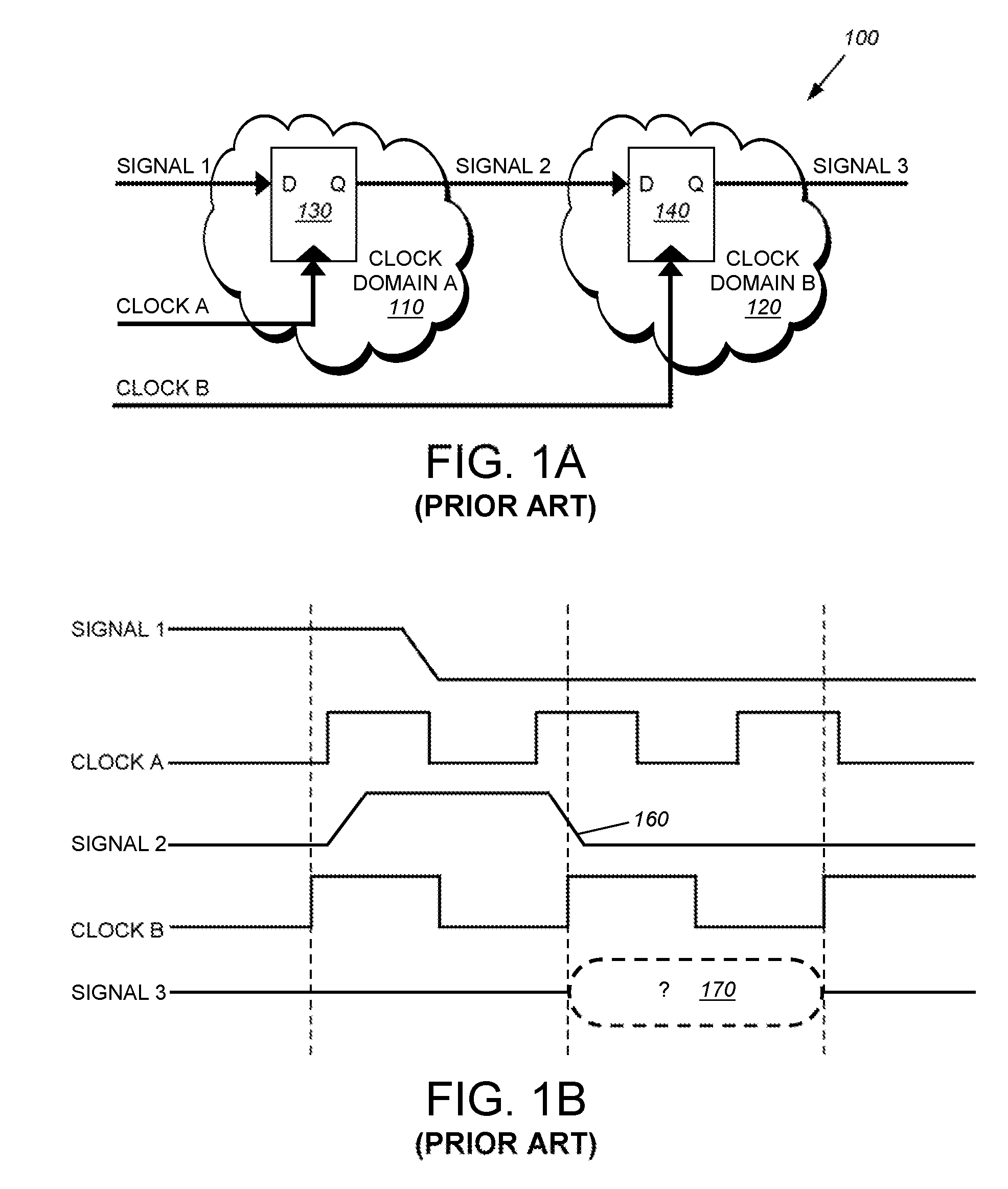
Intercommunication among modules becomes more complex when the modules are driven by clocks from different clock domains, where the clocks of the clock domains are of different families.
Clocks of different families are generally driven by different oscillators and therefore may be considerably out of phase from one another.
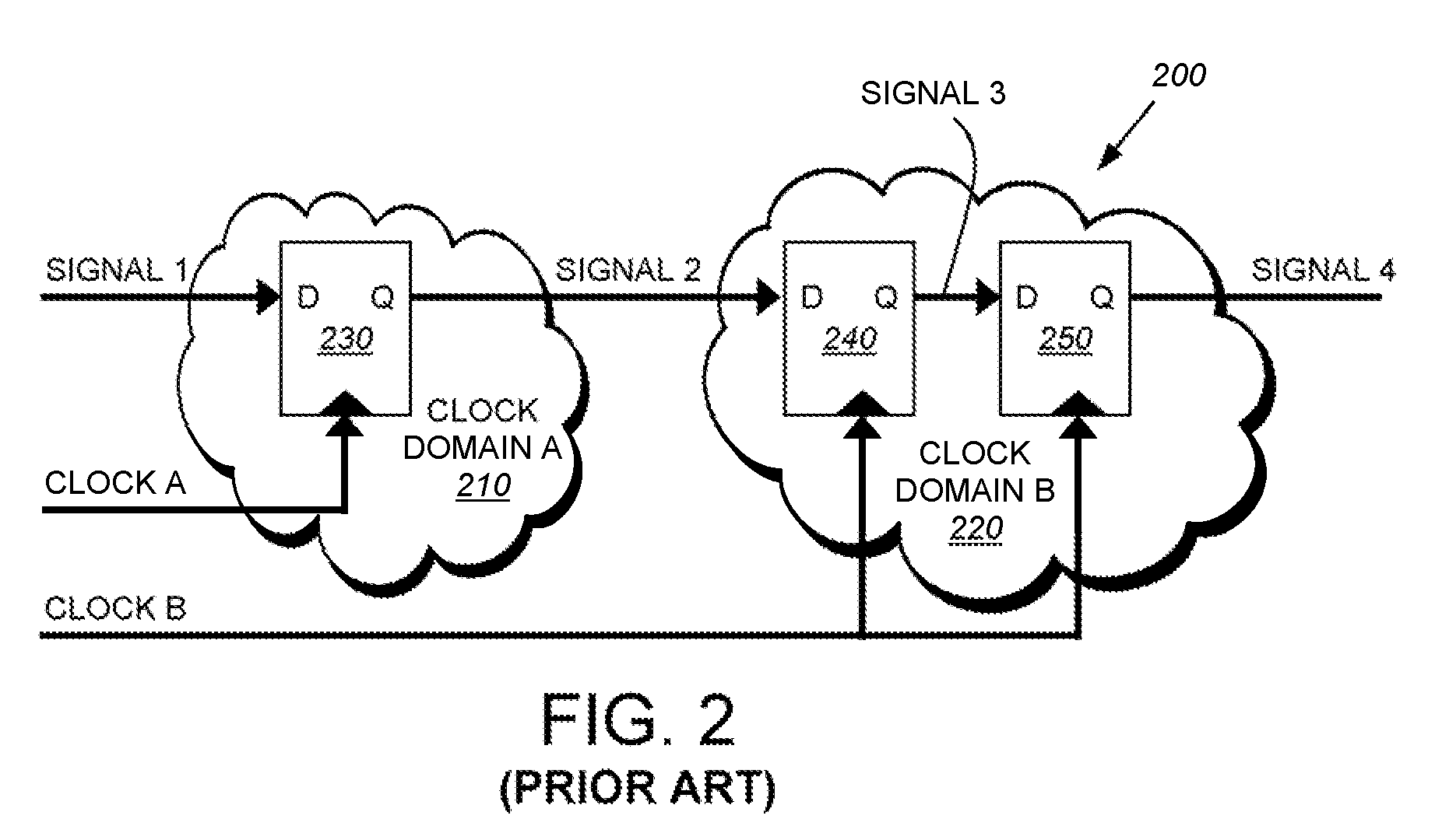
An asynchronous event may cause a flip-flop or other device in the second clock domain to experience metastability, an undesirable unstable state where the device may hold an incorrect value.
Furthermore, metastability may propagate from one device to another device causing a chain of devices to all experience metastability.
As discussed above, this uncertainty is highly undesirable in a hardware design.
As hardware designs become more complex, the burden on the hardware designer to follow good design practices and to explicitly instantiate synchronizers between clock domains increases dramatically.
Indeed, explicit clock synchronization may become untenable as designs continue to increase in size and complexity.
Chip failures due to incorrect implementation of synchronizers are very difficult to detect, as they typically manifest themselves as seemingly random errors and lockups.
Indeed, for an error to manifest itself, a particular combination of clock-edges and data inputs needs to occur.
Such a combination may occur very infrequently and thus detecting such errors may require detailed and exhaustive techniques.
Yet typically many designers attempted to find errors due to incorrect use of synchronizer by visual inspection of the HDL circuit specification and other informal methods.
As is apparent, with the large size of many modern designs, these informal methods are inadequate.
While these tools are an improvement over informal methods, such as visual inspection, they too have their limitations, as described below.
The ability of linting tools to detect clock domain crossing errors is limited due to a number of factors, foremost of which is that conventional HDLs do not well describe how signals are used.
In particular, conventional HDLs generally lack a specific data type for clock signals.
Thus, linting tools may not turn to data types to determine design intent, and are forced to infer intent based upon common design practices and other estimations.
When such inferences are incorrect, linting tool may become confused and thus be unable to recognize certain errors.
Further, since linting tools are generally separate from other design tools and simulators, it is incumbent upon the designer to choose a proper linting tool and to have the discipline to use it at appropriate times. If a designer fails to use an appropriate linting tool, errors will likely be missed, as many other design tools and simulators make little objection to timing errors.

Method used


Image

  • System and method for designing multiple clock domain circuits
  • System and method for designing multiple clock domain circuits
  • System and method for designing multiple clock domain circuits

Examples


Embodiment Construction

[0040]FIG. 4 is a flow diagram 400 that illustrates the synthesis of a TRS circuit specification 410 into a physical hardware device 470. The TRS circuit specification 410 is specified using a plurality of TRS rules that each have a predicate and an action body, and thus may be written in the general form:[0041]π(s)=>s:=δ(s)

where it is the predicate and s:=δ(s) is the action body. Function δ is used to compute the next state of the system from the current state s. The system functions by selecting a rule whose predicate is true, and then atomically (without interaction with other rules) executing the rule's action body. The selecting and executing of rules continues as long as some rule's predicate is true.

[0042]Such a system is suited for design and verification of complex digital systems as explained in Arvind and X. Shen, “Using Term Rewriting Systems to Design and Verify Processors,” MIT LCS Memo CSG-419, IEEE Micro, May / June 1999; Mithal et al., Digital Circuit Synthesis System...


PUM


Abstract

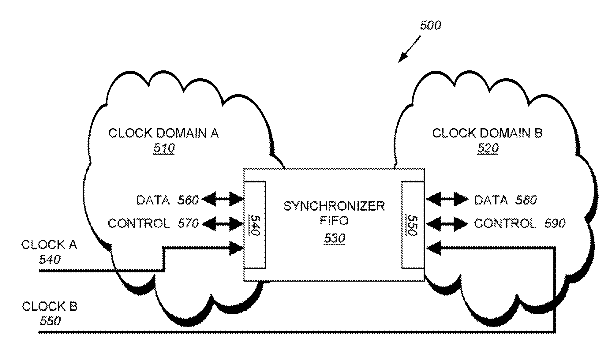
A Hardware Description Language (HDL) utilizing a Term Rewriting System (TRS) is provided that simplifies handling of clocks, and signaling between various clock domains of a multi-clock domain circuit specification. A specific clock data type is supplied for use with clock signals. Using the clock data type, and other requirements of a circuit specification, clock domain crossing between domains of clocks of the same clock family is handled implicitly. For clock domain crossing between clock domains driven by clocks of different clock families, a “hardware approach” and a “linguistic approach” are provided. A “hardware approach” provides facilities to explicitly specify a synchronizer, using, in part, TRS rules. A “linguistic approach” allows a designer to abstracts the instantiation of synchronizers and instead specify a circuit specification in terms of differently clocked interfaces.

Description

RELATED APPLICATIONS[0001]This application is a divisional of U.S. patent application Ser. No. 11 / 448,582, filed Jun. 7, 2006, entitled SYSTEM AND METHOD FOR DESIGNING MULTIPLE CLOCK DOMAIN CIRCUITS, the entire disclosure of which is herein incorporated by reference.FIELD OF THE INVENTION[0002]This invention relates generally to the design and verification of digital circuits, and more specifically, to the design and verification of multiple clock domain digital circuits using a high-level hardware description language.BACKGROUND OF THE INVENTION[0003]Hardware Description Languages (HDLs) have been used for many years to design digital circuits. Such languages employ text-based expressions to describe hardware devices, enabling designers to design larger and more complex systems than possible using previously known gate-level design methods. With HDLs, designers are able to use various constructs to fully describe hardware components and the interconnections between hardware compone...

Claims


Application Information

Patent Timeline
Patent Type & Authority Applications(United States)
IPC IPC(8): G06F17/50
CPCG06F5/06G06F17/5045G06F17/504G06F17/5031G06F30/3323G06F30/3312G06F30/30G06F2117/04
Inventor CZECK, EDWARD W.NANAVATI, RAVI A.NIKHIL, RISHIYUR S.STOY, JOSEPH E.
Owner BLUESPEC
Learn More