
Ten-transistor static random access memory architecture

Inactive Publication Date: 2010-06-10
NATIONAL CHUNG CHENG UNIV
View PDF8 Cites 20 Cited by
  • Summary
  • Abstract
  • Description
  • Claims
  • Application Information

AI Technical Summary

Benefits of technology

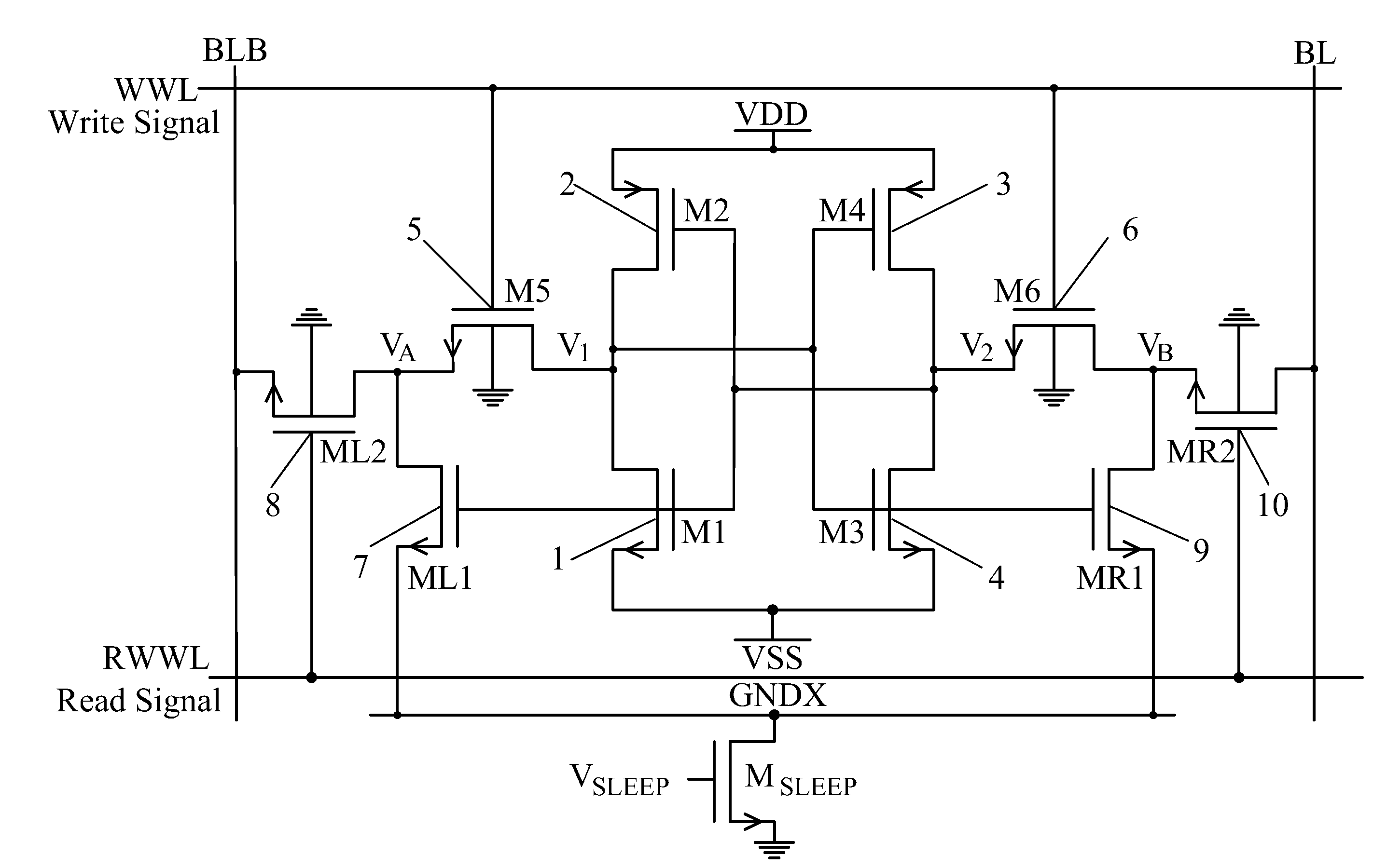
[0009]The 10T SRAM cell of the present invention comprises a memory unit, two data access units, and two noise-immunity units. The memory unit includes two inverters, and each inverter includes a load transistor and a pass transistor. The switching activities of the inverters enable the memory unit to store data. Each of the two data access units contains an access transistor. Each access transistor controls one inverter, whereby the data is accessed via the word line. The two noise-immunity units are respectively arranged beside the two data access units symmetrically and form two symmetric noise-immunity circuit structures at two sides of the memory unit, whereby the memory unit has better noise-immunity capability. Further, the two noise-immunity units connect with the bit lines and word lines and thus provide additional data access paths for the memory unit, whereby the read signals of the bit lines are no more driven by the memory unit. Therefore, the dimensions of the transistors inside the memory unit are no more limited by the required driving capability, and the 10T SRAM architecture can use the minimum-size transistors to achieve a higher operation speed and meet the requirement of the high-speed digital circuit. Further, the 10T SRAM cell of the present invention can achieve an SNM-free feature.

Problems solved by technology

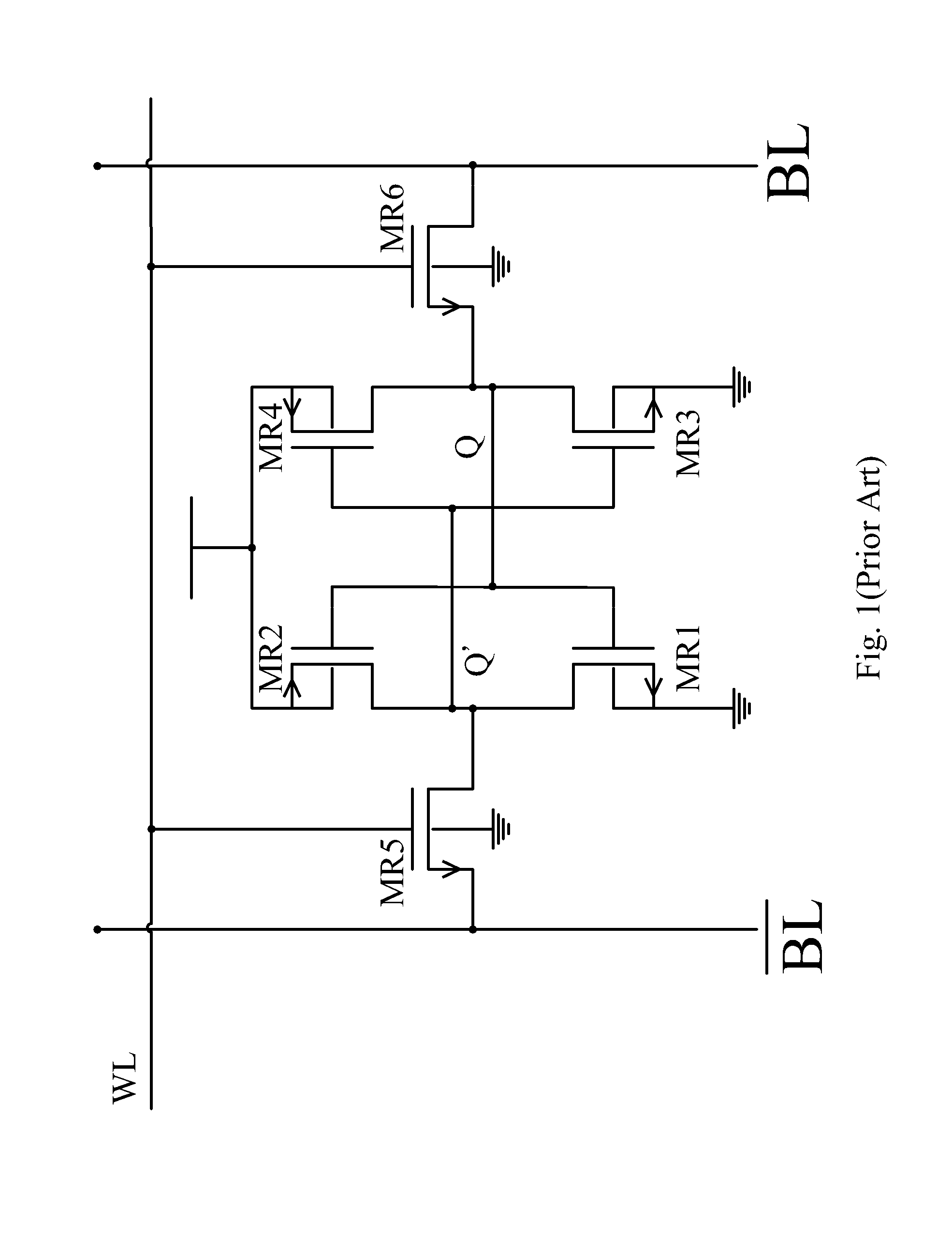
However, the conventional 6T SRAM confronts more and more design difficulties during the evolution of fabrication processes.
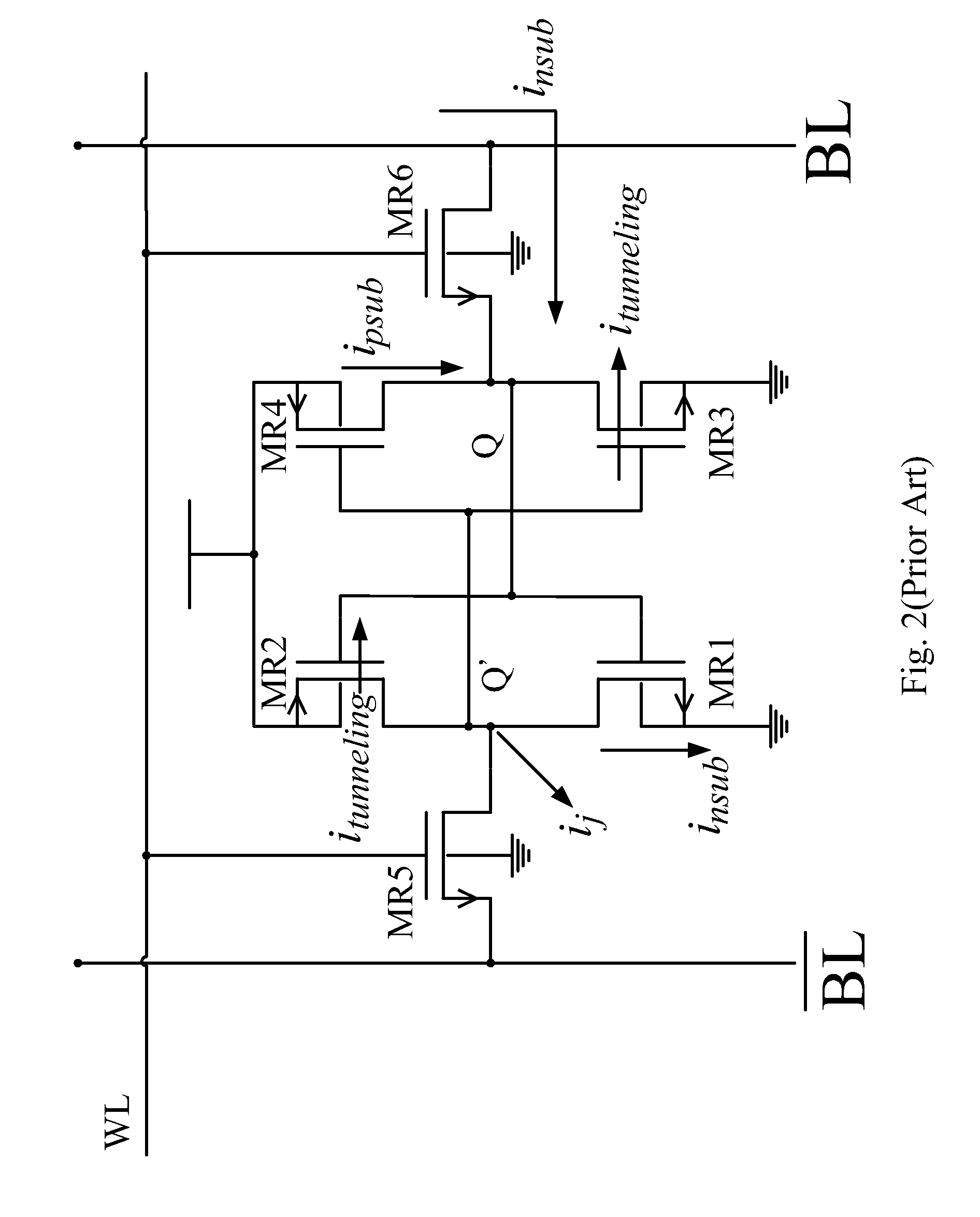
In the advanced processes, the system voltage is decreased persistently, but the leakage current of the gate becomes more serious.
Further, the mismatch caused by process variation is likely to result in instability and access errors in SRAM.
However, a larger memory cell decelerates the output speed.

Method used


Image

  • Ten-transistor static random access memory architecture
  • Ten-transistor static random access memory architecture
  • Ten-transistor static random access memory architecture

Examples


Embodiment Construction

[0014]The present invention discloses a SRAM architecture, particularly a ten-transistor SRAM architecture, which has two additional symmetric data access paths that can also function as the noise-immunity circuit.

[0015]Refer to FIG. 2 for the architecture of a 10T SRAM cell according to the present invention. The 10T SRAM cell of the present invention comprises a memory unit, two data access units, and two noise-immunity units. The memory unit includes two inverters, and each inverter includes a load transistor 1 (or 3) and a pass transistor 2 (or 4). The switching activities of the inverters enable the memory unit to store data. Each of the two data access units contains an access transistor 5 (or 6). Each access transistor 5 (or 6) controls one inverter, whereby the data is accessed via the word line. The two noise-immunity units respectively contain a pair of transistors 7 and 8 and a pair of transistors 9 and 10. The two noise-immunity units are respectively arranged beside the...


PUM


Abstract

The present invention discloses a 10T SRAM architecture, wherein two symmetric data access paths are added to a 6T SRAM architecture. Each data access path has two transistors, whereby the read signals are no more driven by the memory unit, wherefore the dimensions of the transistors inside the 10T SRAM cell are no more limited by the required driving capability. Thus, the 10T SRAM architecture can use the minimum-size transistors to achieve a higher operation speed and meet the requirement of the high-speed digital circuit. Further, the 10T SRAM cell of the present invention can achieve an SNM-free feature.

Description

BACKGROUND OF THE INVENTION[0001]1. Field of the Invention[0002]The present invention relates to a SRAM cell, particularly to a ten-transistor SRAM cell having two additional symmetric data-access paths.[0003]2. Description of the Related Art[0004]SRAM (Static Random Access Memory) is a semiconductor memory and belongs to the RAM family. In SRAM, the stored data will be persistently maintained as long as electricity is held thereinside. Contrarily, the data needs periodically updating in DRAM (Dynamic Random Access Memory). Because of the symmetric circuit structure of SRAM, the data in SRAM can be accessed faster than that in DRAM under same operation frequency. Compare to DRAM where high-address and low-address bits are being read alternately, all bits are read in once within most SRAM which provide higher reading efficiency of SRAM than that of DRAM.[0005]As SRAM far outperforms DRAM in convenience and functions, SRAM is the first choice among RAM for most electronic industries. ...

Claims


Application Information

Patent Timeline
IPC IPC(8): G11C11/00G11C7/00
CPCG11C11/412G11C7/02
Inventor TSAI, TSUNG-HENGGAN, KIAN-ANN
Owner NATIONAL CHUNG CHENG UNIV
Learn More