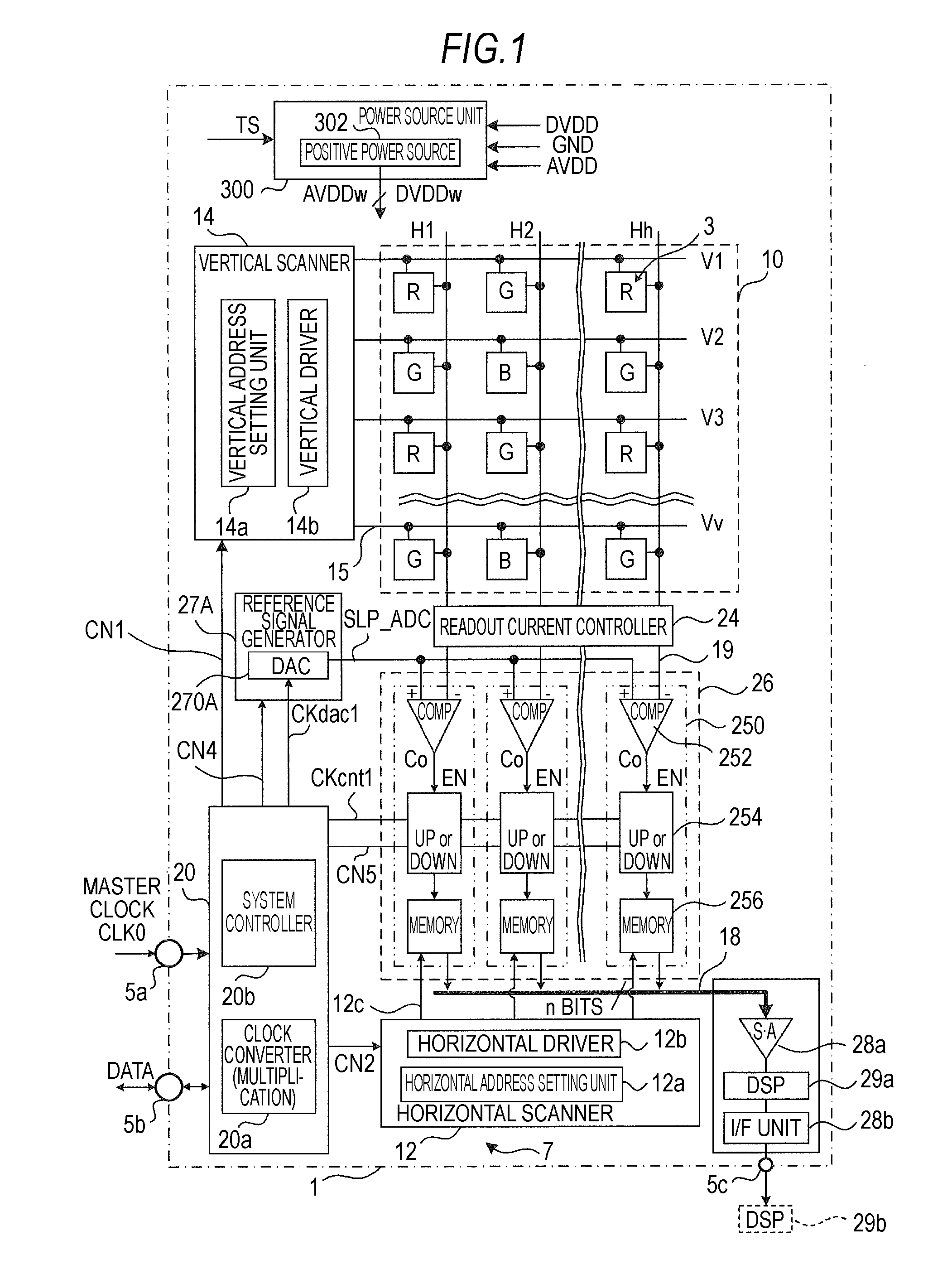
Solid-state imaging device, imaging apparatus, pixel driving voltage adjustment apparatus, and pixel driving voltage adjustment method
a technology of pixel driving voltage and imaging device, which is applied in the direction of color television details, television system details, television systems, etc., can solve problems such as noise generation
- Summary
- Abstract
- Description
- Claims
- Application Information
AI Technical Summary
Benefits of technology
Problems solved by technology
Method used
Image


Examples
verification experiment
[Description of Verification Experiment]
[0097]FIG. 3B shows the driving timing of intermediate transfer and complete transfer in the verification experiment. The horizontal axis represents the time. A shutter time (charge accumulation time) of the complete transfer is Tlsh, a readout time of the complete transfer is Tl, a shutter time (charge accumulation time) of the intermediate transfer is Tssh, and a readout time of the intermediate transfer is Ts. The vertical axis represents the number of output electrons (charge amount). The number of saturated electrons (saturated charge amount) is Qs, the number of retained electrons by the intermediate transfer (intermediate retained charge amount) is Qm, the number of electrons to be read by the intermediate transfer (intermediate transfer charge amount) is Qn, and the number of electrons to be read by the complete transfer (complete transfer charge amount) is Ql.
[0098]The accumulation time ratio Tratio of the intermediate transfer charge...
first embodiment
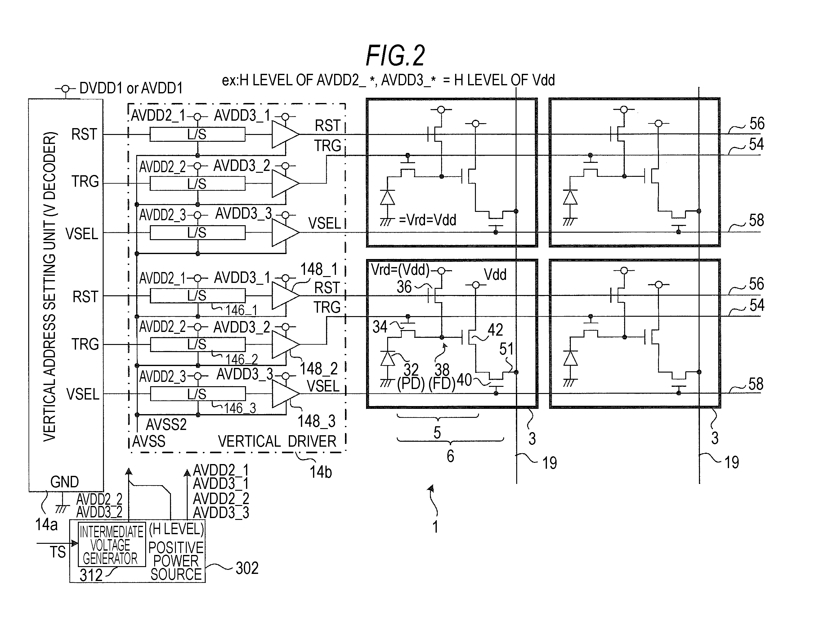
[0106]The first embodiment adopts a scheme in which a charge generator 32 having a saturated charge amount different from the charge generator 32 of the normal pixel is provided in a part of the pixel array unit 10.
[0107]FIGS. 4A and 4B are diagrams illustrating a scheme in which a part of the unit pixel 3 is modified for an intermediate voltage setting adjustment processing of the first embodiment. FIG. 4A is a schematic sectional view illustrating a pixel structure of one pixel. FIG. 4B is a plan view illustrating the structure of the entire pixel array unit 10.
[0108]A charge generator 32 which generates the saturated charge amount Qs with a short exposure time is provided in a part of the pixel array unit 10. A scheme in which the accumulated charge amount of the charge generator 32 is arbitrarily controlled by means other than photoelectric conversion is adopted. This scheme can be easily realized, for example, by physical means that, as shown in FIG. 4A, a member (called a char...
second embodiment
[0130]An intermediate voltage setting adjustment processing of the second embodiment adopts a scheme in which the driving timing is devised to arbitrarily control the charge amount of the charge generator 32. The driving timing also depends on the circuit structure of the unit pixel 3, but basically, it is realized by supplying a voltage, which can saturate the charge generator 32, to the charge generator 32 at a predetermined timing by using a switch unit. A switch transistor (semiconductor device) is turned on at a predetermined timing, so charge injection is performed such that the charge generator 32 is saturated.
[0131]For example, the potential of the floating diffusion 38 is changed, and the potential is notified to the charge generator 32, so the charge amount of the charge generator 32 is adjusted (specifically, forcibly saturated). For this reason, in a state where the pixel power source Vdd is set at the L level, the driving signals of the readout selection transistor 34 a...
PUM
 Abstract
Description
Claims
Application Information
 - R&D
- Intellectual Property
- Life Sciences
- Materials
- Tech Scout
- Unparalleled Data Quality
- Higher Quality Content
- 60% Fewer Hallucinations
Browse by: Latest US Patents, China's latest patents, Technical Efficacy Thesaurus, Application Domain, Technology Topic, Popular Technical Reports.
© 2025 PatSnap. All rights reserved.Legal|Privacy policy|Modern Slavery Act Transparency Statement|Sitemap|About US| Contact US: help@patsnap.com