Liquid crystal display device and a method of manufacturing the same
- Summary
- Abstract
- Description
- Claims
- Application Information
AI Technical Summary
Benefits of technology
Problems solved by technology
Method used
Image
Examples
first embodiment
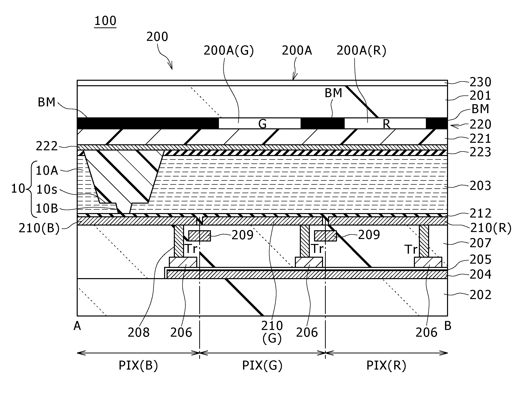
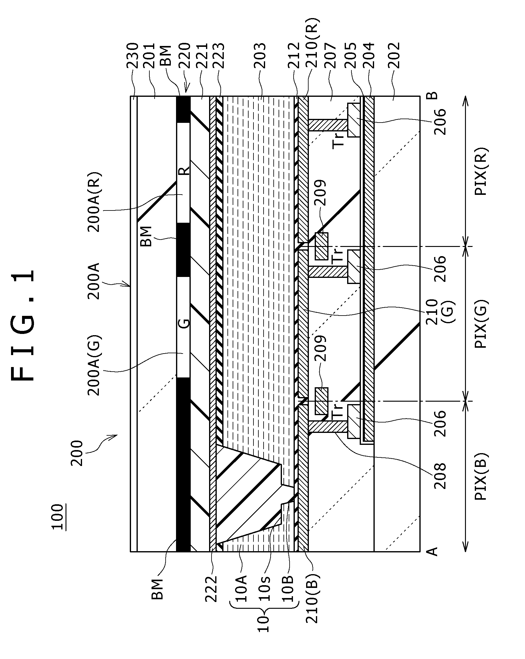
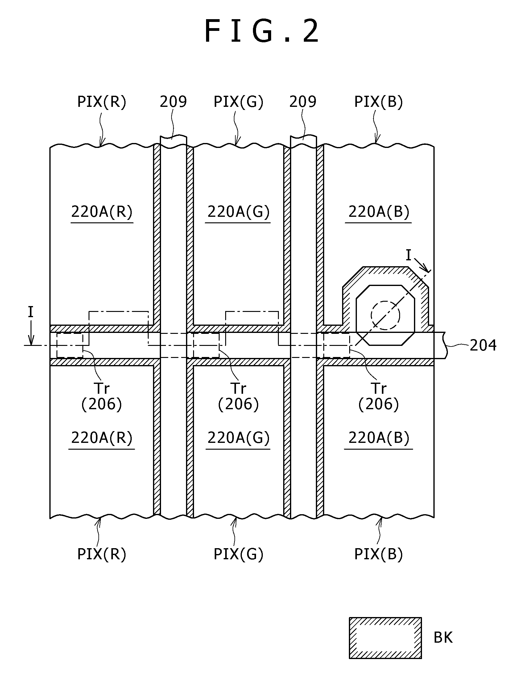
[0046]FIG. 1 is a schematic cross sectional view, showing a structure of a transmission type liquid crystal display device according to a first embodiment of the present invention, taken on line I-I of FIG. 2. FIG. 2 is a simplified plane transparent view showing a part of pixel areas which the transmission type liquid crystal display device of the first embodiment shown in FIG. 1 has.
[0047]The liquid crystal display device 100 illustrated in FIG. 1 has a liquid crystal panel 200, a backlight (not shown), and a drive portion (not shown) for driving the liquid crystal panel 200 and the backlight.
[0048]When viewed from the cross section shown in FIG. 1, in the liquid crystal panel 200, an upper side in FIG. 1 corresponds to “a display surface side,” and a lower side in FIG. 1 corresponds to “a back surface side.” The backlight is disposed on the back surface side so as to be close to the liquid crystal panel 200.
[0049]In the liquid crystal panel 200, a color filter substrate 201 as “a...
second embodiment
[0113]FIGS. 6A to 6E respectively show cross sectional views of the color filter substrate 201 when the spacer 10 having the multiple step structure in a transmission type liquid crystal display device according to the second embodiment of the present invention is manufactured.
[0114]As shown in FIG. 6A, the color filter layer 220 is formed on the color filter substrate 201, and the planarizing film 221 is formed on the color filter layer 220.
[0115]A first level negative resist NR1 is formed on the planarizing film 221 to have a predetermined thickness. Next, as shown in FIG. 6B, by using a photo mask for exposing a portion in which the spacer is intended to be formed of the negative resist NR1 thus formed, and light-blocking the periphery thereof, a negative resist NR portion of the portion in which the spacer is intended to be formed is exposed. As a result, a latent image corresponding to an opening pattern of the photo mask is formed within the negative resist NR1.
[0116]When the ...
third embodiment
[0123]FIGS. 7A and 7E respectively show cross sectional views of the color filter substrate 201 when the spacer 10 having the multiple step structure in a transmission type liquid crystal display device according to the third embodiment of the present invention is manufactured.
[0124]As shown in FIG. 6A, the color filter layer 220 is formed on the color filter substrate 201, and the planarizing film 221 is formed on the color filter layer 220.
[0125]A first level positive resist PR3 is formed on the planarizing film 221 to have a predetermined thickness. Next, as shown in FIG. 7B, by using a photo mask for light-blocking a portion in which the spacer is intended to be formed of the positive resist PR3 thus formed, and exposing the periphery thereof, there is exposed the periphery of a positive resist PR3 portion of the portion in which the spacer is intended to be formed is exposed. As a result, a latent image corresponding to a light-blocking pattern of the photo mask is formed withi...
PUM
 Abstract
Description
Claims
Application Information
 - R&D
- Intellectual Property
- Life Sciences
- Materials
- Tech Scout
- Unparalleled Data Quality
- Higher Quality Content
- 60% Fewer Hallucinations
Browse by: Latest US Patents, China's latest patents, Technical Efficacy Thesaurus, Application Domain, Technology Topic, Popular Technical Reports.
© 2025 PatSnap. All rights reserved.Legal|Privacy policy|Modern Slavery Act Transparency Statement|Sitemap|About US| Contact US: help@patsnap.com


