Semiconductor laser device and manufacturing method thereof

Inactive Publication Date: 2010-03-04
SANYO ELECTRIC CO LTD
View PDF17 Cites 13 Cited by
  • Summary
  • Abstract
  • Description
  • Claims
  • Application Information

AI Technical Summary

Benefits of technology

[0011]The semiconductor laser device according to the first aspect, as described above, includes: the first semiconductor laser element having the first recess extending in the direction in which the first cavity facet extends; and the second semiconductor laser element having the second recess extending in the direction in which the second cavity facet extends, the second cavity facet being formed in substantially the same plane as the first cavity facet. The first and second recesses are therefore formed in substantially the same planes as the first and second cavity facets, respectively. Accordingly, in the manufacturing process thereof, the first cavity facet including a cleavage surface cleaved starting from the first recess of the first semiconductor laser element and the second cavity facet including a cleavage surface cleaved starting from the second recess of the second semiconductor laser element can be aligned in substantially the same plane. In the integrated multi-wavelength semiconductor laser device, it is therefore possible to prevent the cavity facets of the respective semiconductor laser elements from being misaligned in the cavity direction.
[0012]In the semiconductor laser device according to the first aspect, preferably, the second recess extends from a second surface of the second semiconductor laser element to a third surface of the second semiconductor laser element, the second surface opposite side of the second laser element to the first semiconductor laser element, the third surface being bonded to the first semiconductor laser element. In such a configuration, the second recess penetrates the semiconductor element layers of the second semiconductor laser element in the thickness direction. This facilitates cleaving the semiconductor element layers in the manufacturing process. Thus, the second cavity facet can be easily formed.
[0015]In the semiconductor laser device according to the first aspect, preferably, the first recess is formed in a vicinity of a first end of the first cavity facet, in the direction, and the second recess is formed in a vicinity of a second end of the second cavity facet, in the second direction, the second end being on the same side where the first recess is formed. With such a configuration, both the first and second semiconductor laser elements include the recesses (first and second recesses) in the vicinity of the ends of the cavity facets on the same side. Accordingly, unlike the case where the recesses are not formed in the vicinity of the ends of the cavity facets, it is possible to prevent the semiconductor element layers from being broken or cracked in the vicinity of the ends of the cavity facets.
[0016]The manufacturing method of a semiconductor laser device includes: a step of bonding the second semiconductor laser element to a surface of the first semiconductor laser element opposite side of the substrate; and a step of forming a groove for cleavage in a region of the first and second semiconductor laser elements except for at least a region where the first and second optical waveguides are formed, the grooves for cleavage extending in a direction substantially perpendicular to a direction in which the first and second optical waveguides extend; and a step of performing cleavage along the groove for cleavage so as to form the first semiconductor laser element which has a first recess corresponding to the groove for cleavage, the first recess extending in a direction in which the first cavity facet extends, and the second semiconductor laser element which has a second recess corresponding to the groove for cleavage, the second recess extending in a direction in which the second cavity facet extends. Accordingly, the first and second semiconductor laser elements are cleaved starting from the grooves for cleavage, which form the first and second recesses after the cleavage, in the direction substantially perpendicular to the direction in which the first and second optical waveguides extend. Thus, in the first and second semiconductor laser elements, the cavity facets including the cleaved surfaces can be aligned in the cavity direction in substantially the same plane. It is therefore possible to obtain an integrated multi-wavelength semiconductor laser device including cavity facets of the respective semiconductor laser elements prevented from being misaligned in the cavity direction.

Problems solved by technology

However, if the nitride semiconductor laser device and the manufacturing method thereof disclosed in patent literature 1 are applied to a method of fabricating an integrated multi-wavelength semiconductor laser device by bonding multiple semiconductor laser elements to each other, the following problem occurs.
As a result, there is a problem that the cavity facets constituting the three semiconductor elements are misaligned in the cavity direction.
In this case, since the part of laser light is interrupted by the cleaved surface of the adjacent semiconductor laser element, the shape of the beam is abnormal.

Method used


Image

  • Semiconductor laser device and manufacturing method thereof
  • Semiconductor laser device and manufacturing method thereof
  • Semiconductor laser device and manufacturing method thereof

Examples


first embodiment

Modification of First Embodiment

[0087]FIG. 11 is a perspective view showing a structure of a two-wavelength semiconductor laser device according to a modification of the first embodiment. With reference to FIG. 11, in the modification of the first embodiment, a description is given of a case where two-wavelength semiconductor laser device 150 including two wavelength laser elements is formed by bonding red semiconductor laser element 50 to the upper surface of blue-violet semiconductor laser element 160. Note that, blue violet semiconductor laser element 160 is an example of a “first semiconductor laser element” of the invention, and the upper surface of blue-violet semiconductor laser element 160 is an example of the “first surface” of the invention.

[0088]In the modification of the first embodiment, as shown in FIG. 11, in blue-violet semiconductor laser element 160, ridge 165 is formed at a position a predetermined distance (approximately 50 μm, for example) away in the B1 directi...

second embodiment

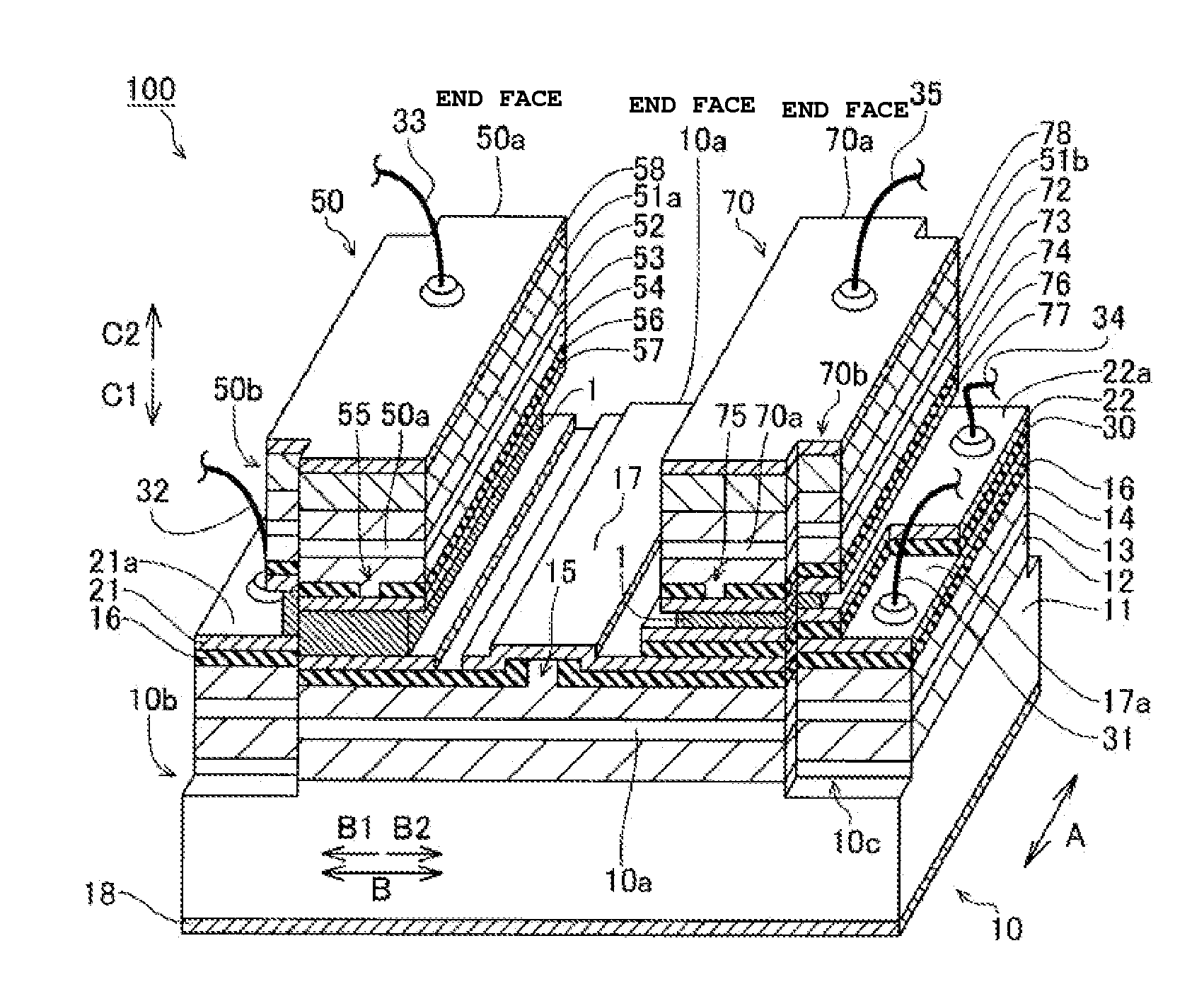
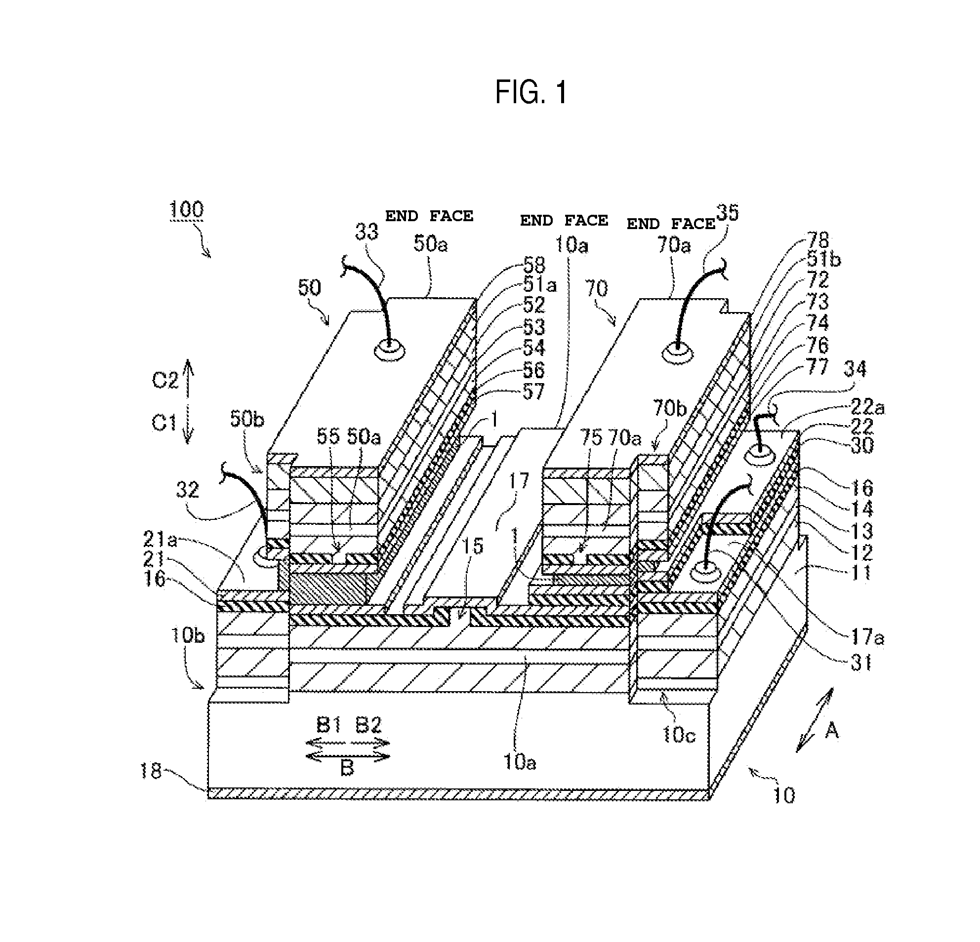
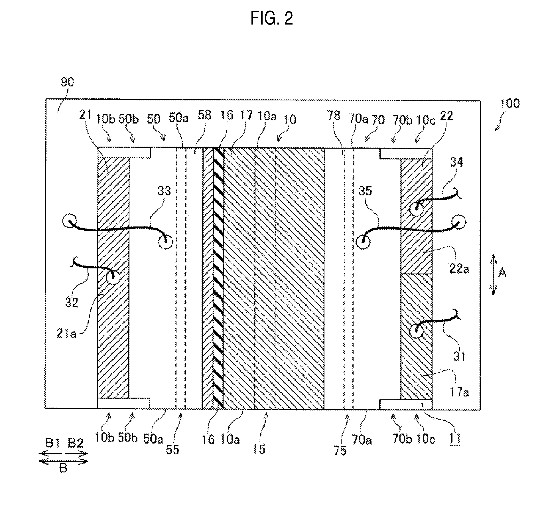
[0093]FIG. 12 is a perspective view showing a structure of a three-wavelength semiconductor laser device according to a second embodiment. FIG. 13 is a view illustrating a manufacturing process of the three-wavelength semiconductor laser device according to the second embodiment shown in FIG. 12. In this second embodiment, with reference to FIGS. 12 and 13, unlike the manufacturing process of the first embodiment, a description is given of a case where scribed grooves formed for bar cleavage of a wafer are separately formed for each semiconductor laser element constituting three-wavelength semiconductor laser device 200.

[0094]In three-wavelength semiconductor laser device 200 according to the second embodiment of the invention, as shown in FIG. 12, red and infrared semiconductor laser elements 50 and 70 are bonded to blue-violet semiconductor laser element 10 with conductive bonding layer 1 interposed therebetween.

[0095]In the second embodiment, recesses 10b and 50b of respective bl...

third embodiment

[0101]FIG. 14 is a perspective view showing a structure of a three-wavelength semiconductor laser device according to a third embodiment. FIG. 15 is a view illustrating a manufacturing process of the three-wavelength semiconductor laser device according to the third embodiment shown in FIG. 14. In this third embodiment, with reference to FIGS. 14, a description is first given of a case where three-wavelength semiconductor laser device 300 is formed by bonding blue-violet semiconductor laser element 10 to monolithic two-wavelength semiconductor laser element 310 having red and infrared semiconductor laser elements 50 and 70 integrally formed into a single body, unlike the first embodiment.

[0102]As shown in FIG. 14, in three-wavelength semiconductor laser device 300 according to the third embodiment, monolithic two-wavelength semiconductor laser element 310, which includes red and infrared semiconductor laser elements 50 and 70 formed on a lower surface of n-type GaAs substrate 311 at...


PUM


Abstract

A first semiconductor laser element is formed on a surface of a substrate and has a first cavity facet. The first semiconductor laser element has a first recess in the first cavity facet except for at least a region where a first optical waveguide is formed. The first recess extends in a first direction in which the first cavity facet extends. A second semiconductor laser element is bonded to a first surface of the first semiconductor laser element. The first surface is arranged opposite side of the first laser element to the substrate, and has a second cavity facet formed in substantially the same plane as the first cavity facet. The second semiconductor laser element has a second recess in the second cavity facet except for a region where a second optical waveguide is formed, the second recess extending in a second direction in which the second cavity facet extends.

Description

CROSS REFERENCE TO RELATED APPLICATIONS[0001]This application claims priority based on 35USC119 from prior Japanese Patent Application No. P2008-216186 filed on Aug. 26, 2008, entitled “SEMICONDUCTOR LASER DEVICE AND MANUFACTURING METHOD THEREOF”, the entire contents of which are incorporated herein by reference.BACKGROUND OF THE INVENTION[0002]1. Field of the Invention[0003]The invention relates to a semiconductor laser device and a manufacturing method thereof, and in particular, relates to a semiconductor laser device including integrated semiconductor laser elements and a manufacturing method thereof.[0004]2. Description of Related Art[0005]A conventional semiconductor laser device including optical waveguides is disclosed in, for example, Japanese Patent Application Publication No. 2003-17791 (herein referred to as patent literature 1)[0006]Patent literature 1 discloses a nitride semiconductor laser device including nitride compound semiconductor layers formed on a GaN substrat...

Claims


Application Information

Patent Timeline
IPC IPC(8): H01S5/026H01L21/30
CPCB82Y20/00H01S5/4087G11B7/22H01S5/0202H01S5/0217H01S5/0224H01S5/02272H01S5/028H01S5/0425H01S5/1082H01S5/22H01S5/2214H01S5/34313H01S5/34326H01S5/34333H01S5/4043G11B7/1275H01L2224/48463H01L2224/73265H01S5/04256H01S5/0234H01S5/02345H01S5/0237
Inventor BESSHO, YASUYUKI
Owner SANYO ELECTRIC CO LTD
Why Eureka
Try Eureka