
Method of online predicting maintenance of an apparatus

a maintenance method and technology of an apparatus, applied in the direction of optical radiation measurement, instruments, spectrometry/spectrophotometry/monochromators, etc., can solve the problems of difficult process use, increased cost of each individual wafer, and strict requirements for semiconductor wafer manufacturing processes

Active Publication Date: 2010-02-18
BEIJING NAURA MICROELECTRONICS EQUIP CO LTD
View PDF11 Cites 7 Cited by
  • Summary
  • Abstract
  • Description
  • Claims
  • Application Information

AI Technical Summary

Benefits of technology

[0010]The object of the present invention is to provide a convenient method to online predict maintenance and replacement of components of apparatus, which can predict the period of maintenance and replacement of components of apparatus effectively and accurately without changing the apparatus or adding any additional components.
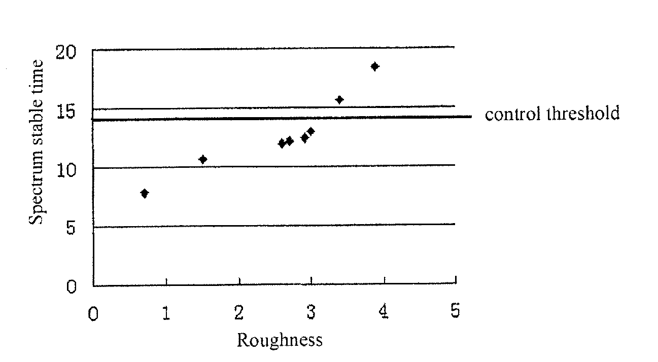
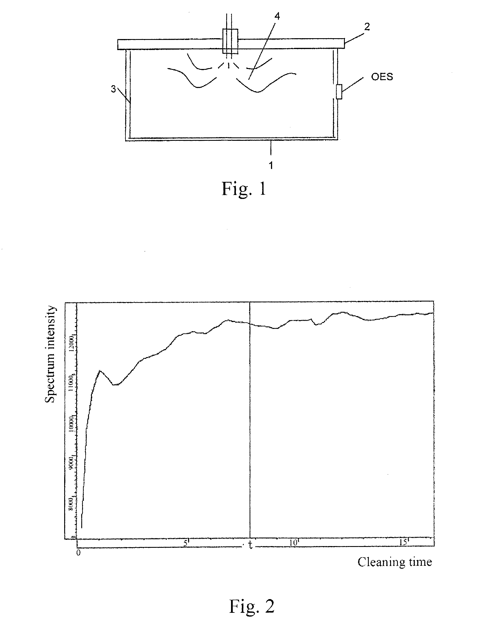
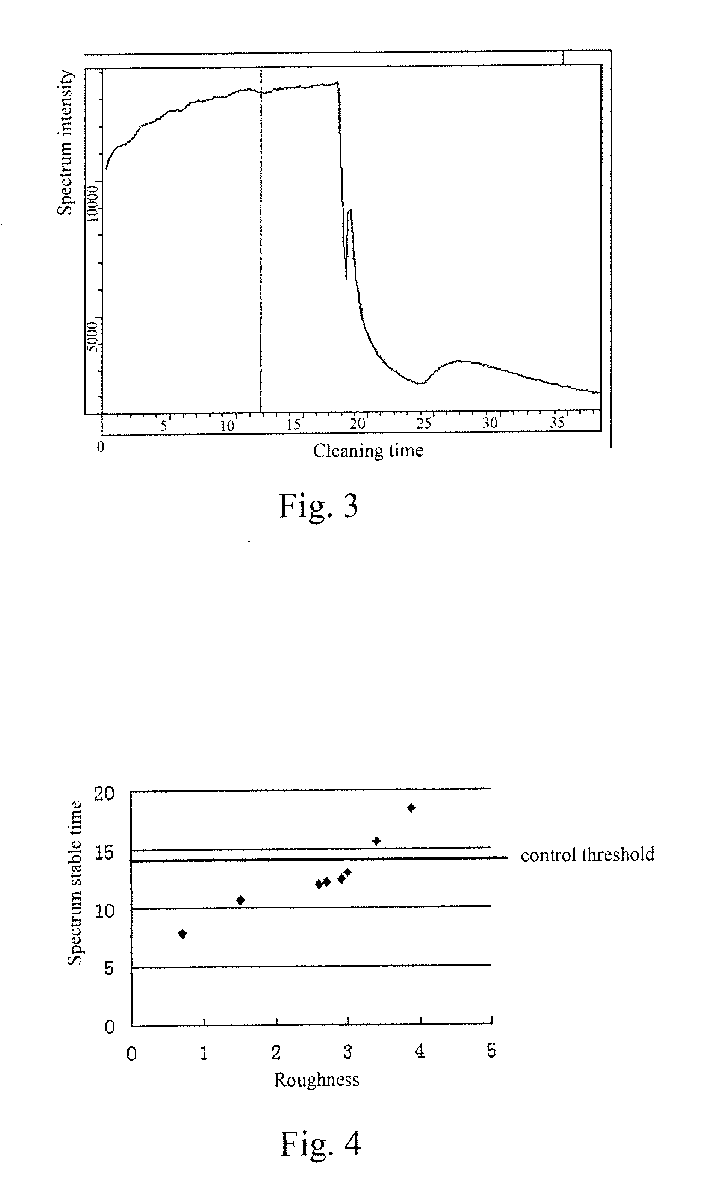
[0016]From the above technical solutions provided by the present invention, it can be seen that the method of present invented online predicting maintenance of the apparatus uses an inherent OES sensor mounted on the apparatus, and uses OES to detect the change in the intensity of the spectrum emitted in the process; and quantifies the process parameter in the process, according to the analysis to results detected; and by statistically analyzing the spectrum intensity detected and quantified many times, obtains the function relationship of process parameters with the spectrum intensity; then performs a maintenance operation, when the quantified value of the process parameter exceeds a control threshold set according to the requirements of the process to the apparatus. The present invention avoids not only frequent shutdown or the process drift because of insufficient maintenance due to the inaccuracy of conventional maintenance period estimated experimentally; but also changing the apparatus or addition of any other additional online sensor, thereby decreasing cost. The production efficiency of processing substrates (such as silicon wafer) is increased and the waste substrates caused by fault process result are avoided, therefore the yield is improved.

Problems solved by technology

As a result, the cost of each individual wafer is increasing, and the requirements to the semiconductor wafer manufacturing process are stricter.
However it is difficult to use in a process wherein feature size is less than 90 nm.
Using this method, the apparatus maintenance period can be estimated only by experience, and it is difficult to predict which part of the apparatus needs to be maintained accurately and quantitatively.
Very long period will result in that the change in the working condition in process causes the change in processing result, thus leading to the degrading of wafer quality, and reducing the throughput rate; on the other hands, very short period will lead to frequent maintenance, which will affect disadvantageously regular wafer process, and result in wasting time and decreasing of efficiency.
The disadvantages of the conventional methods mentioned above are that the cost of apparatus is increased, and the mechanical design of apparatus is needed to change so as to satisfy the additional sensor.

Method used


Image

  • Method of online predicting maintenance of an apparatus
  • Method of online predicting maintenance of an apparatus
  • Method of online predicting maintenance of an apparatus

Examples


embodiment 1

[0034]The roughness of the quartz window 2 and liner 3 surfaces will increase under the bombardment of plasma 4, thereby their surfaces will no longer be smooth. With the process proceeds, the surfaces will be rougher and rougher. The roughness refers to that: the surface is not entirely smooth, forming microcosmic topography of small spaced-apart peak and valley. Generally, the roughness is measured by the Roughness Tester. Moving the Roughness Tester on a surface of an object to be detected for a certain distance, the roughness of the object can be obtained by calculating the average distance between peak and valley on the path of the tester. When the inner surface of each component are exposed in the chamber, by-products of the process will be attached to the inner surface, and these by-products will become gaseous during dry clean process after each regular process and be extracted. Thus, during dry clean process, monitoring the amount of the products or the reactants will obtai...

embodiment 2

[0044]The replacement of the OES window may be predicted by means of the change of OES spectrum intensity during regular processes, wherein a certain distance exists between the OES window and the plasma. This method deals mainly with the OES window. By-products will fall on the surface of OES window during the process and this position is hard to be cleaned in dry clean process, thus the OES spectrum intensity will gradually decrease with the times of the process being repeated increasing. Therefore the changing trend of average value of the OES spectrum in regular process is measured and a control threshold is set, so when the average value goes below the control threshold, it means that the OES window has been polluted and should be replaced. Thus, the replacement of OES window can be predicted by detecting the change of OES spectrum intensity.

[0045]FIG. 5 shows the relationship between the number of substrates (such as silicon wafers) processed with the intensity of the emitted ...


PUM


Abstract

A method of online predicting maintenance of an apparatus is disclosed. Using an optical emission spectroscopy (OES) positioned on the apparatus and the change of emission spectrum intensity detected by the OES in the process, according to the detected results, measuring the parameter in the process, the function relation between the process parameter and spectrum intensity is acquired. A control threshold is decided by the processing requirement to the apparatus. When the parameter exceeds the control threshold, maintenance to the etching apparatus is engaged in order to avoid processing error caused by frequent shutdown or deficient maintenance which is estimated by experience, and hence decreasing the cost and increasing processing efficiency of substrates (such as silicon wafers) without changing apparatus and adding other online sensor, and improving production rate by avoiding waste substrates caused by error processing results. The method is suitable for semiconductor substrate etching maintenance of the apparatus and also other maintenance of the apparatus.

Description

BACKGROUND OF THE INVENTION[0001]1. Field of the Invention[0002]The present invention relates, generally, to a method of predicting maintenance of an apparatus, and, more particularly, to a method of online predicting maintenance of an apparatus.[0003]2. Description of the Related Art[0004]With the improvement of semiconductor chip technology, the feature size is keeping decreased from 250 nm to 65 nm, even less than 45 nm; while the size of silicon wafer is increased from 200 mm to 300 mm. As a result, the cost of each individual wafer is increasing, and the requirements to the semiconductor wafer manufacturing process are stricter. The semiconductor manufacturing comprises many process steps including deposition, photolithography and etching process, etc., wherein the etching process is more complex, because the state of plasma and other parameters during the etching process have direct influence upon the result of etching process. With the feature size decreasing, it is more and ...

Claims


Application Information

Patent Timeline
IPC IPC(8): G06F11/30
CPCH01L21/67253
Inventor CHEN, ZHUOHU, LIQIONGXIE, KAI
Owner BEIJING NAURA MICROELECTRONICS EQUIP CO LTD
Learn More