Electro-Optic Crystal-Based Structures and Method of Their Fabrication

a technology of electrooptic crystals and crystal structures, applied in the field of optical and electrooptical devices, can solve problems such as not expected to manifest gradual deterioration in performance, and achieve the effects of low refractive index, high optical quality, and index of refraction

Inactive Publication Date: 2010-02-18
YISSUM RES DEV CO OF THE HEBREWUNIVERSITY OF JERUSALEM LTD +1
View PDF3 Cites 0 Cited by
  • Summary
  • Abstract
  • Description
  • Claims
  • Application Information

AI Technical Summary

Benefits of technology

[0027]The inventor has found that the amorphous regions (i.e. regions of the amorphous KLTN-based material) having lower refractive indices can be fabricated by implantation of light ions (such as H30, D+, He++ carbon, oxygen) at energies of several MeVs into the KLTN-based crystal. Such an implantation allows for creating well defined layer(s) of the amorphous material, having high optical quality and index of refraction typically 5%-10% lower than that of the crystal in which these layers are formed.
[0028]The inventor has also found that unlike KTN, where the electro-optic response slows down in the vicinity of the phase transition where the effect is large, in KLTN fast electro-optic response can be obtained while maintaining a large electro-optic effect by increasing the Li concentration.
[0042]According to yet another aspect of the invention, there is provided a method of processing of a KLTN-based material, the method comprising at least one of the following: (a) bombarding said KLTN-based material with light ions; (b) etching said KLTN-based material when in amorphous state by an acid; thereby allowing fabrication of one or more optical components within the KLTN-based material.

Problems solved by technology

KLTN crystal was found to be a chemically inert, non-hygroscopic and stable material, so that it is not expected to manifest gradual deterioration in performance.

Method used


Image

  • Electro-Optic Crystal-Based Structures and Method of Their Fabrication
  • Electro-Optic Crystal-Based Structures and Method of Their Fabrication
  • Electro-Optic Crystal-Based Structures and Method of Their Fabrication

Examples


Embodiment Construction

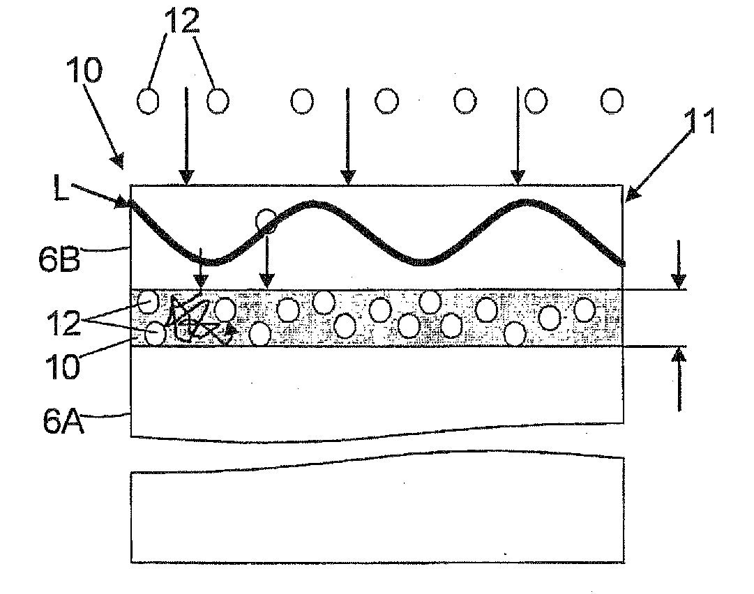
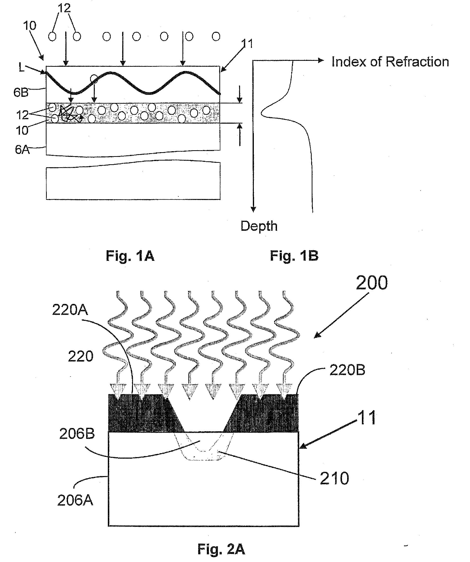
[0056]Referring to FIG. 1A, there is shown an example of an optical structure 100 of the present invention for use in optic and electro-optic devices. Structure 100 includes a region 10 of an amorphous KLTN-based material, enclosed between lower and upper regions 6A and 6B of a crystalline KLTN-based material 11. In the present example, amorphous region 10 and crystalline region 6B are designed to have refractive indices and thicknesses enabling effective waveguiding propagation) of a beam L of some light wavelength(s) and polarization(s) along region 6B. Amorphous region 10 presents a boundary (cladding) defining a waveguide region 6B enclosed between said cladding and the upper surface of structure 100 serving as the opposite boundary.

[0057]Amorphous region 10 is formed by implantation of light ions, generally at 12, into the KLTN substrate 11. Regions (layers) 6A and 6B are portions of the substrate separated by layer 10 resulted from the implantation. Interfaces between layers 6...


PUM

PropertyMeasurementUnit
electric fieldaaaaaaaaaa
feature sizeaaaaaaaaaa
widthaaaaaaaaaa

Abstract

A structure is presented for use in optic and electro-optic devices. The structure comprises at least one region of an amorphous KLTN-based material in a KLTN-based material. Also provided is a method of processing a KLTN-based material, comprising at least one of the following: bombarding said KLTN-based material with light ions: and etching said KLTN-based material when in amorphous state by an acid; thereby allowing fabrication of one or more optical components within the KLTN-based material.

Description

FIELD OF THE INVENTION[0001]This invention relates to optical and electro-optical devices and methods of their fabrication.REFERENCES[0002]The following references are considered to be pertinent for the purpose of understanding the background of the present invention:[0003]1. J. Y. C. Wong, L. Zhang, G. Kakarantzas, P. D. Townsend, and P. J. Chandler, “Ion-implanted optical waveguides in KTaO3”, J. Appl. Phys. 71 (1), 49-52, 1 Jan. 1992.[0004]2. D. Fluck, R. Gutmann, and P. Günter, “Optical waveguides in KTa1-xNbxO3 produced by He ion implantation”, J. Appl. Phys. 70 (9), 5147-5149, 1 Nov. 1991.[0005]3. F. P. Strohkendl and P. Günter, “Formation of optical waveguides in KNbO3, by low dose MeV He+ implantation”, J. Appt. Phys. 69 (1), 84-88, 1 Jan. 1991.[0006]4. A. J. Agranat, R. Hofmeister and A. Yariv, “Characterization of a New Photorefractive Material: K1-yLiyTa1-xNbxO3”, Optics Letters 17, 713 (1992).[0007]5. A. J. Agranat, L. Secundo, N. Golshani, and M. Razvag, “Wavelength Sel...

Claims


Application Information

Patent Timeline
Patent Type & Authority Applications(United States)
IPC IPC(8): G02B6/00G03F7/20
CPCB82Y20/00G02B6/1347G02F1/225G02F1/31G02B1/02G02F2202/20G02F2202/32G02F2203/15C23C14/48G02F2201/307
Inventor AGRANAT, AHARON
Owner YISSUM RES DEV CO OF THE HEBREWUNIVERSITY OF JERUSALEM LTD
Why Eureka
Try Eureka