
Hybrid heterojunction solar cell fabrication using a doping layer mask

a technology of heterojunction and solar cells, applied in the field of photovoltaic cell fabrication, can solve the problems of prior manufacturing methods and add to the cost of solar cell completion, and achieve the effect of preventing substantial etching of the back surfa

Inactive Publication Date: 2010-01-21
APPLIED MATERIALS INC
View PDF46 Cites 123 Cited by
  • Summary
  • Abstract
  • Description
  • Claims
  • Application Information

AI Technical Summary

Benefits of technology

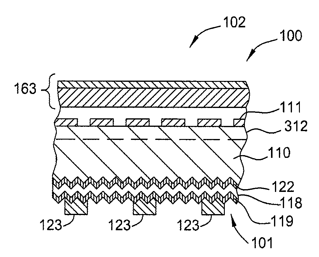
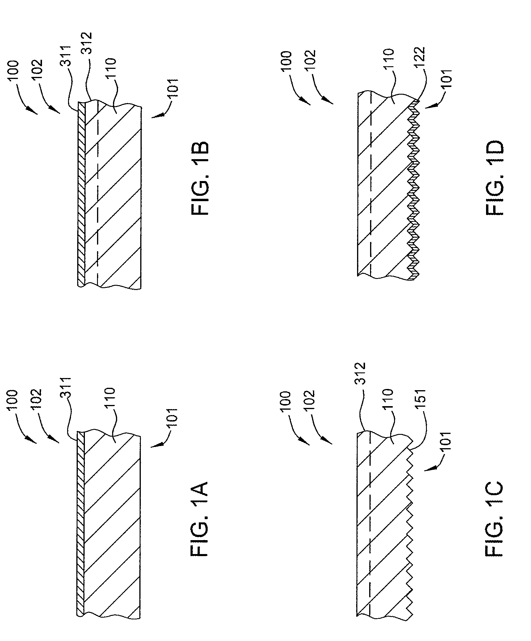
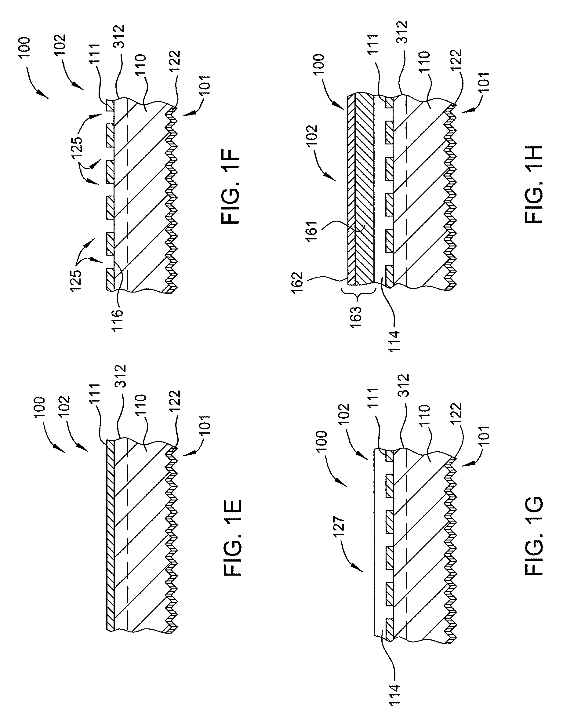
[0009]In one embodiment, the present invention generally provides a method of forming a solar cell device, comprising forming an amorphous silicon layer on a back surface of a crystalline silicon substrate, and texturing a front surface of the crystalline silicon substrate, wherein the amorphous silicon layer disposed on the back surface is configured to prevent substantial etching of the back surface during the process of texturing the front surface.

Problems solved by technology

However, there are several issues with these prior manufacturing methods.
For example, the formation processes are complicated multistep processes that add to costs required to complete the solar cells.

Method used


Image

  • Hybrid heterojunction solar cell fabrication using a doping layer mask
  • Hybrid heterojunction solar cell fabrication using a doping layer mask
  • Hybrid heterojunction solar cell fabrication using a doping layer mask

Examples


Embodiment Construction

[0022]Embodiments of the invention contemplate the formation of a high efficiency solar cell using a novel processing sequence to form a solar cell device. In one embodiment, the methods include the use of various etching and patterning processes that are used to define active regions of the device and regions where the device and / or contact structure is to be located on a surface of a solar cell substrate. The method generally includes the steps of forming one or more layers on a backside of a solar cell substrate to protect the backside of the substrate from being attacked during the subsequent process, and provide a stable supporting surface when the front side regions of the solar cell are formed. Solar cell substrates (e.g., substrate 110 in FIG. 1A) that may benefit from the invention include substrates that may have an active region containing organic material, single crystal silicon, multi-crystalline silicon, polycrystalline silicon, germanium (Ge), gallium arsenide (GaAs),...


PUM

PropertyMeasurementUnit
Temperatureaaaaaaaaaa
Electrical conductivityaaaaaaaaaa
Efficiencyaaaaaaaaaa

Abstract

Embodiments of the invention contemplate the formation of a high efficiency solar cell using a novel processing sequence to form a solar cell device. In one embodiment, the methods include forming a doping layer on a back surface of a substrate, heating the doping layer and substrate to cause the doping layer diffuse into the back surface of the substrate, texturing a front surface of the substrate after heating the doping layer and the substrate, forming a dielectric layer on the back surface of the substrate, removing portions of the dielectric layer from the back surface to from a plurality of exposed regions of the substrate, and depositing a metal layer over the back surface of the substrate, wherein the metal layer is in electrical communication with at least one of the plurality of exposed regions on the substrate, and at least one of the exposed regions has dopant atoms provided from the doping layer.

Description

CROSS-REFERENCE TO RELATED APPLICATIONS[0001]This application claims benefit of U.S. Provisional Patent Application Ser. No. 61 / 081,362 [Attorney Docket #: APPM 13438L], filed Jul. 16, 2008, and Provisional Patent Application Ser. No. 61 / 121,537 [Attorney Docket #: APPM 13438L02], filed Dec. 10, 2008, which are both herein incorporated by reference in their entirety. This application also relates to U.S. patent application Ser. No. ______ [Attorney Docket #: APPM 13438], filed Jul. 16, 2009.BACKGROUND OF THE INVENTION[0002]1. Field of the Invention[0003]Embodiments of the invention generally relate to the fabrication of photovoltaic cells.[0004]2. Description of the Related Art[0005]Solar cells are photovoltaic devices that convert sunlight directly into electrical power. The most common solar cell material is silicon, which is in the form of single or multicrystalline substrates, sometimes referred to as wafers. Because the amortized cost of forming silicon-based solar cells to gen...

Claims


Application Information

Patent Timeline
IPC IPC(8): H01L21/20H01L21/28C23F1/00
CPCH01L21/67155H01L31/022425Y02E10/50H01L31/1876H01L31/0236Y02P70/50
Inventor WEIDMAN, TIMOTHY W.MISHRA, ROHITSTEWART, MICHAEL P.CHA, YONGHWA CHRISWIJEKOON, KAPILA P.FANG, HONGBIN
Owner APPLIED MATERIALS INC
Learn More