Semiconductor device

a technology of semiconductor film and shielding circuit, which is applied in the direction of emergency protective circuit arrangement, emergency protective circuit arrangement for limiting excess voltage/current, basic electric elements, etc., can solve the problem of limited kind of protection circuit including lateral diodes, and achieve the effect of improving the performance of protection circuit including diodes formed using semiconductor films and reducing wiring resistan

Inactive Publication Date: 2010-01-14
SEMICON ENERGY LAB CO LTD
View PDF14 Cites 15 Cited by
  • Summary
  • Abstract
  • Description
  • Claims
  • Application Information

AI Technical Summary

Benefits of technology

[0167]FIG. 24A is a plan view of the semiconductor film 405 included in the amplifier circuit 302. FIG. 24B is a layout diagram of the semiconductor film 405 and the first conductive film 410. The semiconductor film 405 in the photodetector 300 is L-shaped as illustrated in FIG. 24A, and the outer shape of the semiconductor film 405 is rectangular in this embodiment. In addition, in the amplifier circuit 302, a plurality of semiconductor films 480 are formed in addition to the semiconductor film 405. The semiconductor films 480 are dummy semiconductor films and are not used for transistors. By forming the semiconductor film 480, the following advantageous effects can be obtained: the thickness of a conductive film formed above the semiconductor film 405 is made uniform and etching is uniformly performed on the conductive film.
[0168]FIG. 24C is a plan view of the diode 321. In this embodiment, the positions of the n-type impurity region 401 and the p-type impurity region 402 are opposite to those of the diode 321 in Embodiment 5. Note that FIG. 24C also illustrates the openings 431 through which the n-type impurity region 401 and the conductive film 411 are connected to each other and the openings 432 through which the p-type impurity region 402 and the conductive film 411 are connected to each other.
[0169]FIG. 25 is a plan view of the second conductive films 411 to 414. In this embodiment, the shape of the conductive film 411 is improved so that wiring resistance of the plurality of transistors 306 in a first stage of the amplifier circuit 302 is equivalent to wiring resistance of the first terminal 11. Since the conductive film 411 includes twelve branch points which correspond to connection portions for connection to the amplifier circuit 302 in regions surrounded by dashed-dotted lines, the wiring width of portions to which the branch points are connected is gradually narrowed from a direction away from the connection portions for connection to the first terminal 11 to a direction close to the connection portions for connection to the first terminal 11 (from left to right in the diagram). In addition, a bend portion 411a is formed in part of the branch points so that the length of wiring is increased. The conductive film 412 is similar to the conductive film 411. The wiring width of portions to which the twelve branch points are connected is gradually narrowed from a direction away from the connection portions for connection to the second terminal 12 to a direction close to the connection portions for connection to the second terminal 12 (from right to left in the diagram). In addition, a bend portion 412a is formed in part of the branch points so that the length of wiring is increased. By forming the conductive film 411 and the conductive film 412 in this manner, in the case where overvoltage is transiently applied to the power supply terminal 311 or the power supply terminal 312 due to ESD or the like, voltage can be prevented from being applied to mainly one transistor 305 or 306 in the amplifier circuit 302. Thus, the possibility of damage to the amplifier circuit 302 can be lowered.
[0170]FIG. 26 illustrates the layout of the third conductive films 421 and 422 and the fourth conductive film 461. FIG. 26 also illustrates the openings 471 and 472 formed in the sealing film 510 and the openings 473 and 474 formed in the silicon nitride oxide film 509.
[0171]In the photodetector 330 of this embodiment, the second conductive films 411 and 412 are provided so that resistance of a plurality of current paths between the amplifier circuit 302 and the power supply terminal 311 and resistance of a plurality of current paths between the amplifier circuit 302 and the power supply terminal 312 are made uniform. Accordingly, high voltage can be prevented from being applied to the amplifier circuit 302, so that resistance of the amplifier circuit 302 itself to ESD is improved. That is, according to this embodiment, combined with improvement in performance of the protection circuit 320, even though unexpected overvoltage is applied to the terminal due to ESI) or the like, the possibility of damage to the amplifier circuit 302 can be further lowered.
[0172]Needless to say, the usage of this embodiment is not limited to photodetectors. In this embodiment, since connection wirings (second conductive films) are used for part of the functions of a protection circuit, the protection circuit can be easily made smaller. Thus, it is preferable to apply this embodiment to a small semiconductor device having a size less than or equal to 10 mm×10 mm. Note that the semiconductor device having the size less than or equal to 10 mm×10 mm is a semiconductor device which is provided in a region of 10 mm×10 mm in the layout.Embodiment 7

Problems solved by technology

However, in Reference 1, the kind of the protection circuit including the lateral diode is limited to a certain kind.
Further, the technique disclosed in Reference 2 is not a technique for improving resistance of the circuit itself to ESD but a technique for normally operating the circuit even after the PIN diode is damaged.

Method used


Image

  • Semiconductor device
  • Semiconductor device
  • Semiconductor device

Examples


embodiment 1

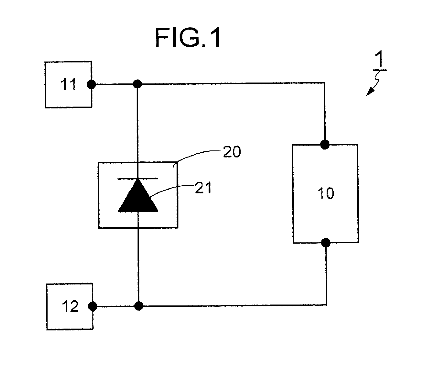
[0046]First, a semiconductor device according to this embodiment is described with reference to FIG. 1. FIG. 1 is a block diagram illustrating a structural example of the semiconductor device of this embodiment.

[0047]As illustrated in FIG. 1, a semiconductor device 1 of this embodiment includes a circuit 10 including a plurality of semiconductor elements, a first terminal 11, a second terminal 12, and a protection circuit 20. The circuit 10 is electrically connected to the first terminal 11 and the second terminal 12. The first terminal 11 and the second terminal 12 are an output terminal and / or an input terminal of the semiconductor device 1 and are connection portions for connection to a different semiconductor device. For example, each of the first terminal 11 and the second terminal 12 serves as a power supply terminal, a signal output terminal, or a signal input terminal.

[0048]The protection circuit 20 is a circuit for preventing overvoltage from being applied to the circuit 10...

embodiment 2

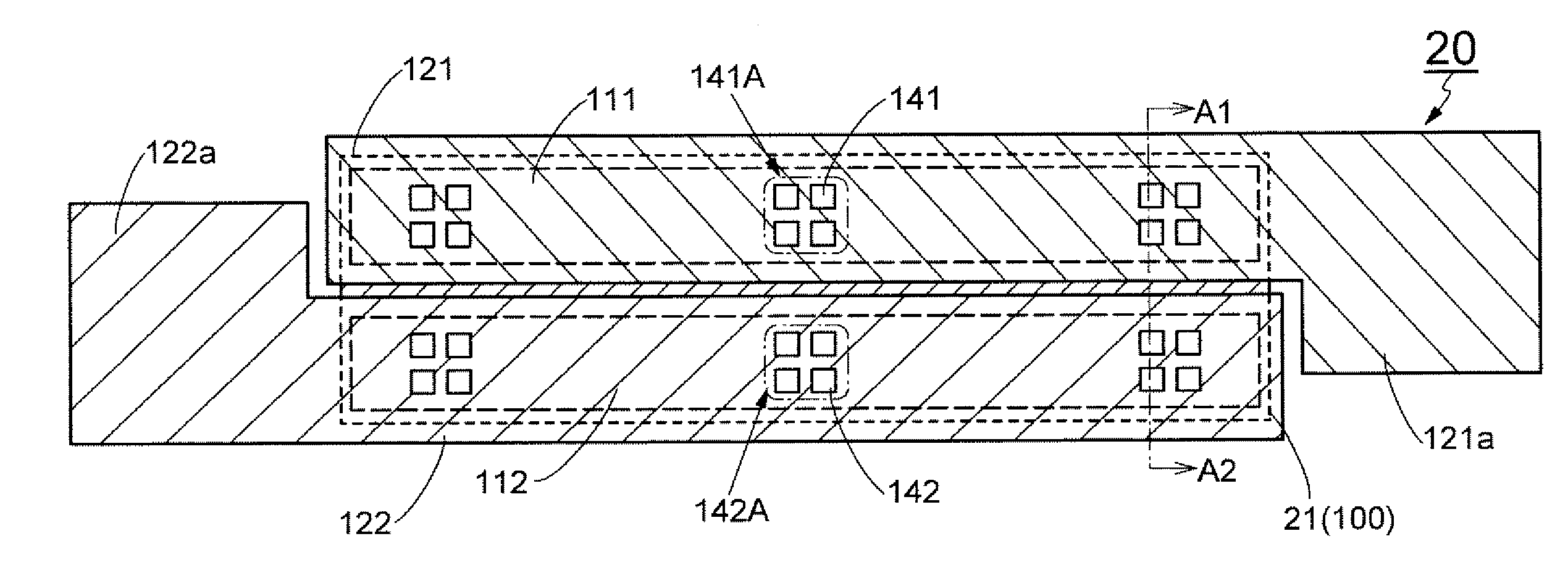
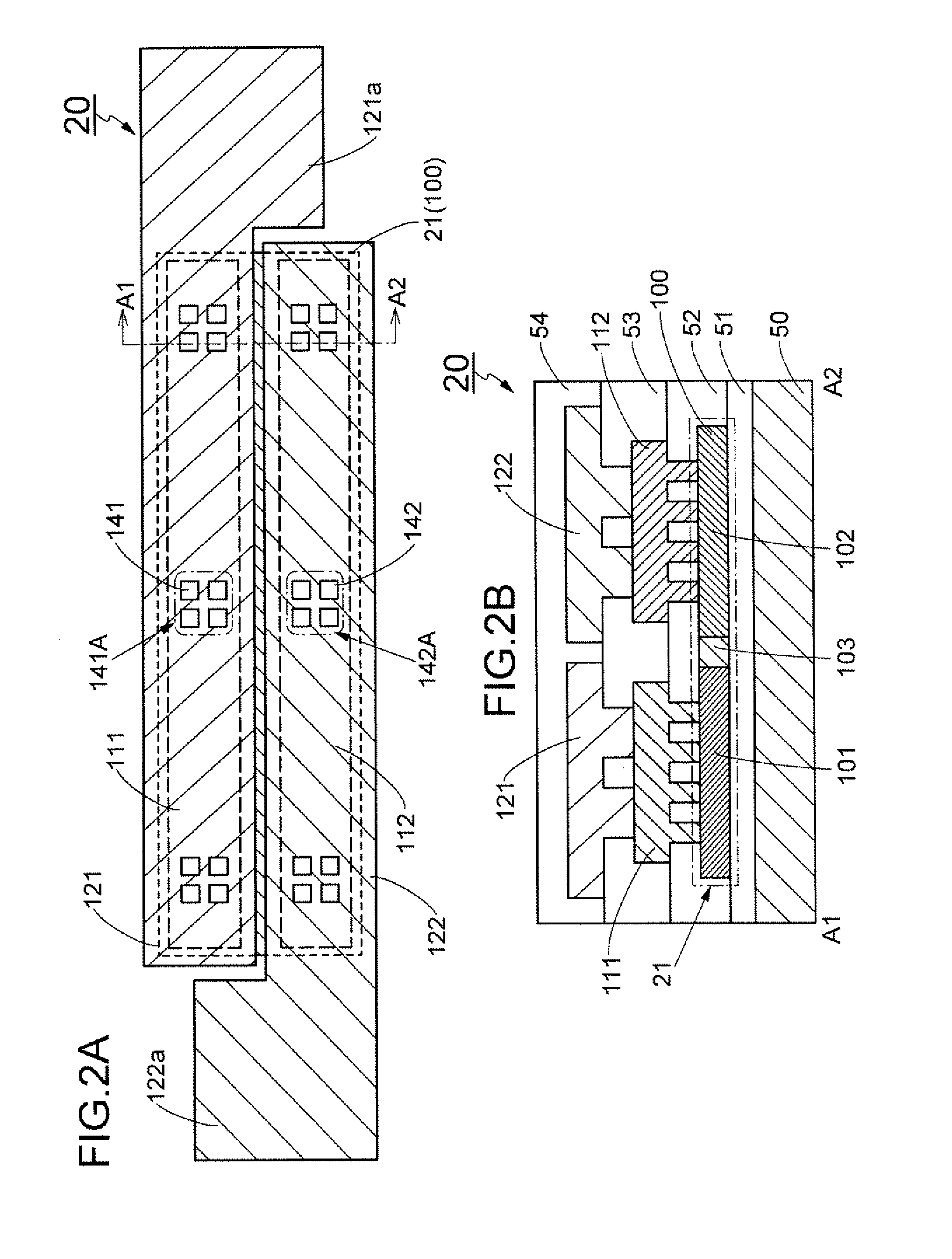
[0078]In this embodiment, different structural examples of the first conductive films 111 and 112 in the protection circuit 20 (see FIG. 2A) are described. The first conductive films 111 and 112 can be formed using a conductive film which is the same as a conductive film used for an internal wiring (or an internal electrode) of the circuit 10. FIG. 5A is a plan view of a protection circuit including such conductive films. Here, in order to distinguish this protection circuit from the protection circuit 20 in FIG. 2A, this protection circuit is referred to as a protection circuit 25. Needless to say, the protection circuit 25 can be used as the protection circuit 20 in FIG. 1 and FIGS. 4A to 4C. Further, the layered structure of the protection circuit 25 is similar to the layered structure of the protection circuit 20 (see FIG. 1).

[0079]FIG. 5B is a layout diagram of a semiconductor film and a first conductive film in the protection circuit 25. As illustrated in FIG. 5B, a first cond...

embodiment 3

[0082]In this embodiment, a technique for increasing the bond length of a diode without increasing the size of a semiconductor film used for the diode is described. In this embodiment, three structural examples of protection circuits are described with reference to FIGS. 6A to 6C, FIGS. 7A to 7C, and FIGS. 5A to 8C. Here, in order to distinguish the protection circuits in the three structural examples described in this embodiment from the protection circuit 20 (FIGS. 2A and 2B) and the protection circuit 25 (FIG. 5A), these protection circuits are referred to as protection circuits 31 to 33. Diodes which are used in the protection circuits 31 to 33 are referred to as diodes 41 to 43.

[0083]In addition, in this embodiment, an example is described in which a conductive film including a portion which serves as the internal wiring of the circuit 10 is used as a first conductive film in each of the protection circuits 31 to 33, in a manner similar to that of the protection circuit 25 in F...


PUM


Abstract

To improve the performance of a protection circuit including a diode formed using a semiconductor film. A protection circuit is inserted between two input / output terminals. The protection circuit includes a diode which is formed over an insulating surface and is formed using a semiconductor film. Contact holes for connecting an n-type impurity region and a p-type impurity region of the diode to a first conductive film in the protection circuit are distributed over the entire impurity regions. Further, contact holes for connecting the first conductive film and a second conductive film in the protection circuit are dispersively formed over the semiconductor film. By forming the contact holes in this manner wiring resistance between the diode and a terminal can be reduced and the entire semiconductor film of the diode can be effectively serve as a rectifier element.

Description

BACKGROUND OF THE INVENTION[0001]1. Field of the Invention[0002]The present invention relates to a semiconductor device including a means for preventing a circuit from being damaged by application of unexpected high voltage due to electrostatic discharge or the like.[0003]2. Description of the Related Art[0004]One of major causes of defects in integrated circuits is damage of semiconductor elements, electrodes, or the like due to electrostatic discharge (hereinafter referred to as ESD). Thus, in order to prevent an integrated circuit from being damaged due to ESD, a protection circuit is inserted between a terminal and the integrated circuit. A protection circuit refers to a circuit for preventing overvoltage or overcurrent generated due to ESD from being supplied to an integrated circuit. Typical examples of elements used for protection circuits are resistors, diodes, capacitors, and the like.[0005]For example, in References 1 and 2, a technique by which a diode is formed using a s...

Claims


Application Information

Patent Timeline
IPC IPC(8): H01L29/04
CPCH01L27/0255H01L27/1214H01L27/12H01L27/1262H01L27/1277
Inventor FUKUOKA, OSAMUHAYAKAWA, MASAHIKOSHISHIDO, HIDEAKI
Owner SEMICON ENERGY LAB CO LTD
Why Eureka
Try Eureka