Bidirectional switch having control gate embedded in semiconductor substrate and semiconductor device

a technology of semiconductor substrate and control gate, which is applied in the direction of semiconductor devices, basic electric elements, electrical appliances, etc., can solve the problems of unstable threshold voltage vt, drain resistance of each unidirectional semiconductor element, and degradation of gate insulating film quality, so as to reduce on-resistance, improve heat dissipation properties near current paths, and improve gate insulating films quality

Inactive Publication Date: 2010-01-07
RENESAS ELECTRONICS CORP
View PDF0 Cites 4 Cited by
  • Summary
  • Abstract
  • Description
  • Claims
  • Application Information

AI Technical Summary

Benefits of technology

[0014]The configuration described above allows a region between a trench gate of the first switch and a trench gate of the second switch to be formed by a well region which also serves as a drain, so that the heat dissipation properties near a current path are improved. Moreover, the configuration eliminates the need for forming trenches large in width, and thus trenches each having a flat bottom portion can be formed. Accordingly, the quality of the gate insulating films is improved.
[0015]The present invention can provide a bidirectional switch element with reduced on-resistance and a constant threshold voltage, and a semiconductor device.

Problems solved by technology

Each of these unidirectional semiconductor elements, however, has drain resistance.
Forming each of the trenches 33 with a large width makes it difficult to obtain a flat bottom portion of the trench 33, thereby deteriorating the quality of the gate insulating films 36 formed in the trench 33.
These cause problems of making a threshold voltage Vt unstable and on-resistance high.
Moreover, in Patent Document, the two separate gate electrodes 37 need to be formed in each of the trenches 33, which makes a process complicated.

Method used


Image

  • Bidirectional switch having control gate embedded in semiconductor substrate and semiconductor device
  • Bidirectional switch having control gate embedded in semiconductor substrate and semiconductor device
  • Bidirectional switch having control gate embedded in semiconductor substrate and semiconductor device

Examples


first exemplary embodiment

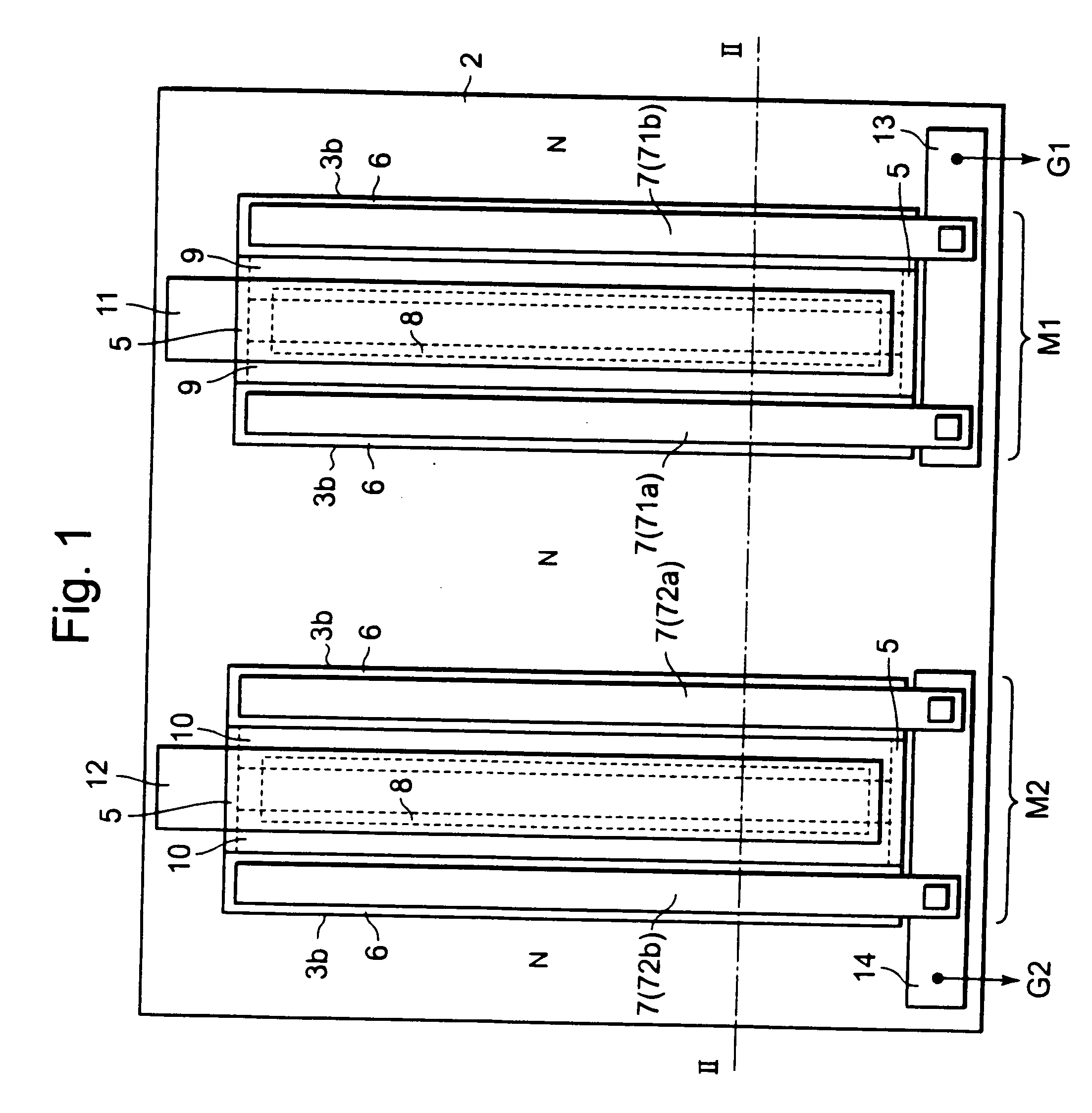
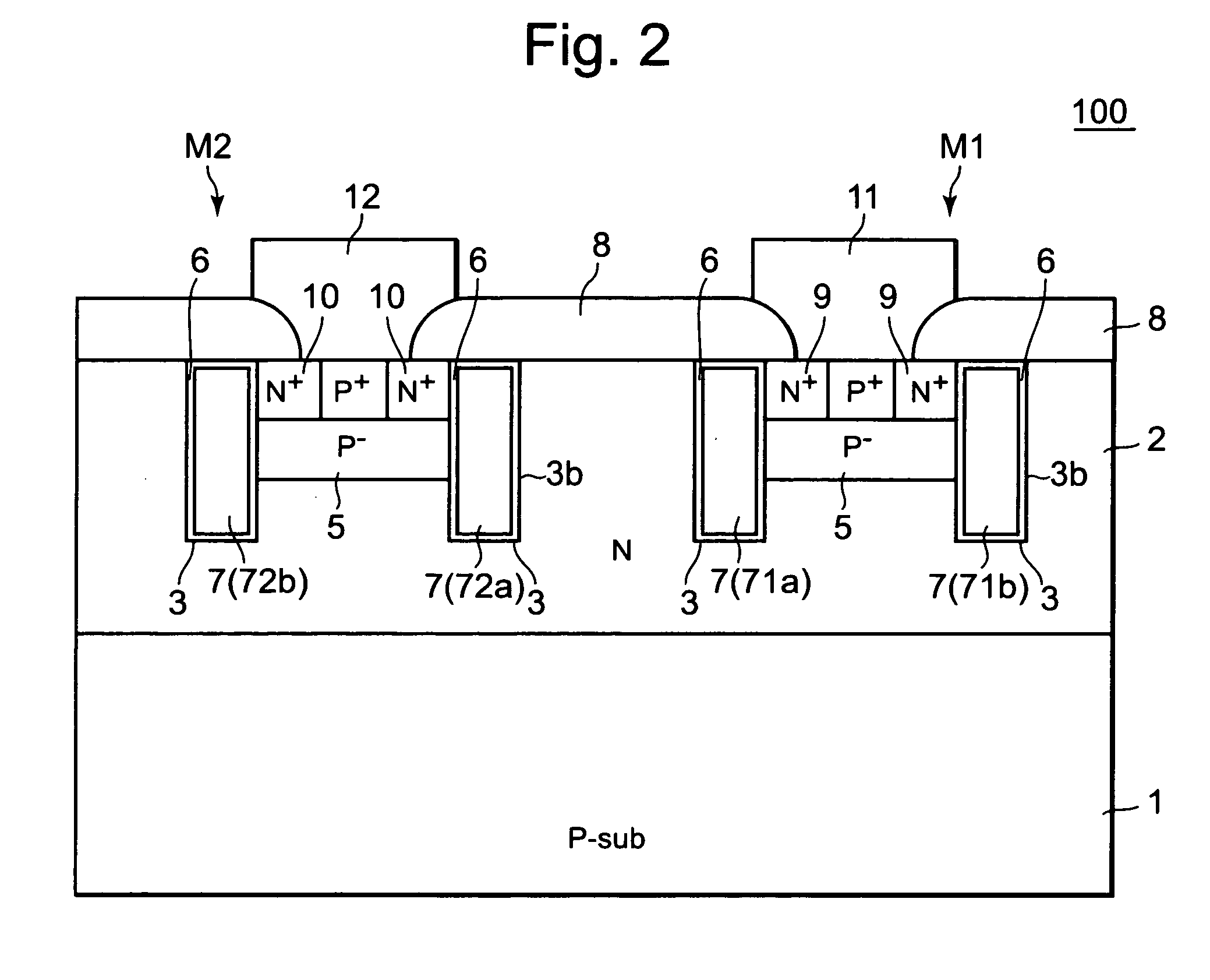
[0022]FIG. 1 is a plan view of the bidirectional switch 100 according to a first exemplary embodiment. FIG. 2 is a cross-sectional view of the bidirectional switch 100 according to the first exemplary embodiment. FIG. 2 shows a cross-sectional view taken along II-II line of FIG. 1. The bidirectional switch 100 is a bidirectional semiconductor element provided with a first MOS switch M1 and a second MOS switch M2, as shown in FIG. 1 and FIG. 2.

[0023]In FIG. 1 and FIG. 2, an N-well region 2 having an impurity concentration of a 30 predetermined level is formed on a P-semiconductor substrate 1. Trenches 3 are formed in the N-well region 2 at predetermined intervals. In the exemplary embodiment, four trenches 3 are formed. Gate insulating films (gate oxide films) 6 are respectively formed on side walls 3b of the trenches 3.

[0024]Inside each of the trenches 3, a gate electrode 7 is formed with the gate insulating film interposed in between. In other words, the trenches 3 are each provide...

second exemplary embodiment

[0044]FIG. 4 is a cross-sectional view of the bidirectional switch 100 according to a second exemplary embodiment. FIG. 4 shows, as in FIG. 2, a cross-sectional view taken along II-II line of FIG. 1.

[0045]As shown in FIG. 4, an N+ embedded diffusion layer 4 is further formed between a P-semiconductor substrate 1 and an N-well region 2. The N+ embedded diffusion layer 4 has an impurity concentration higher than that of the N-well region 2. The configuration other than this point is the same as that of the first exemplary embodiment, thereby omitting the description thereof. This configuration improves separation between elements from each other, in addition to the same effects as those of the first exemplary embodiment.


PUM


Abstract

A bidirectional switch includes a first switch and a second switch. The switch includes a well region of a first-conductivity-type formed on a semiconductor substrate, and serving as drains of the first switch and the second switch, a gate electrode of the first switch provided in a first trench formed in the well region through a first gate insulating film, a gate electrode of the second switch formed in a second trench formed in the well region so as to be spaced apart from the first trench with a second gate insulating film, a source region of the first switch formed on a side wall of the first trench, and on a surface of the well region via a first channel region of a second-conductivity-type, and a source region of the second switch formed on a side wall of the second trench, and on a surface of the well region via a second channel region of the second-conductivity-type. The well region is formed in a region between the first trench and the second trench.

Description

INCORPORATION BY REFERENCE[0001]This application is based upon and claims the benefit of priority from Japanese Patent Application No. 2008-175524 which was filed on Jul. 4, 2008, the disclosure of which is incorporated herein in its entirety by reference.BACKGROUND OF THE INVENTION[0002]1. Field of the Invention[0003]The present invention relates to a bidirectional switch and a semiconductor device, particularly to a bidirectional switch capable of controlling switching in each of two directions individually, and to a semiconductor device.[0004]2. Description of Related Art[0005]A power unit, for example, for a lithium ion battery performs controls for both charging and discharging of the lithium ion battery, in order to avoid excessive charging and discharging of the lithium ion battery. To this end, required is a semiconductor device provided with a bidirectional switch which allows electric currents to flow in two directions. For more accurate charging and discharging, the semic...

Claims


Application Information

Patent Timeline
Patent Type & Authority Applications(United States)
IPC IPC(8): H01L29/747
CPCH01L27/0705H01L29/7813H01L29/7397H01L29/0878
Inventor YANAGIGAWA, HIROSHI
Owner RENESAS ELECTRONICS CORP
Why Eureka
Try Eureka