Electron-emitting device, method of manufacturing the same, electron source, and image display apparatus
- Summary
- Abstract
- Description
- Claims
- Application Information
AI Technical Summary
Benefits of technology
Problems solved by technology
Method used
Image
Examples
example 1
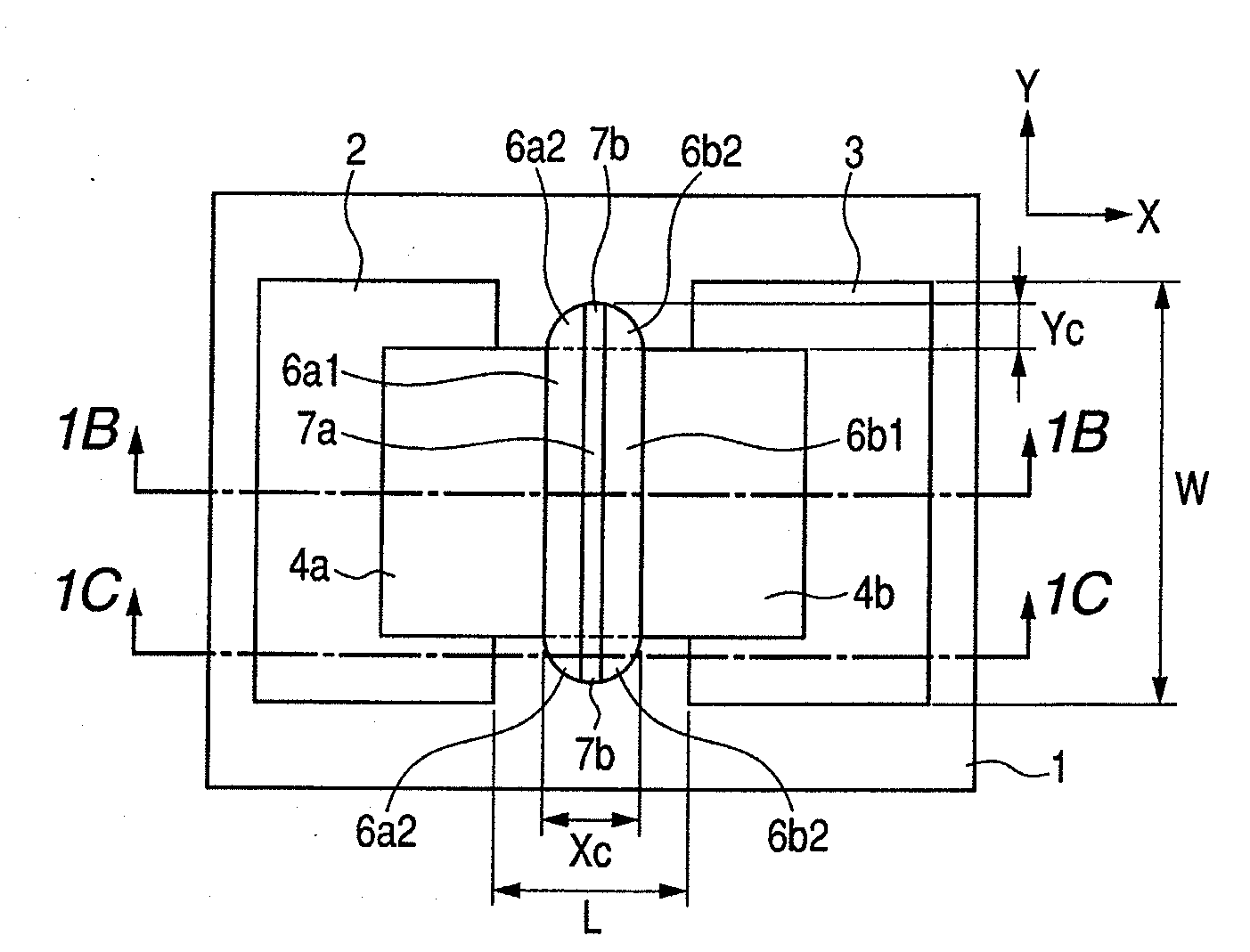
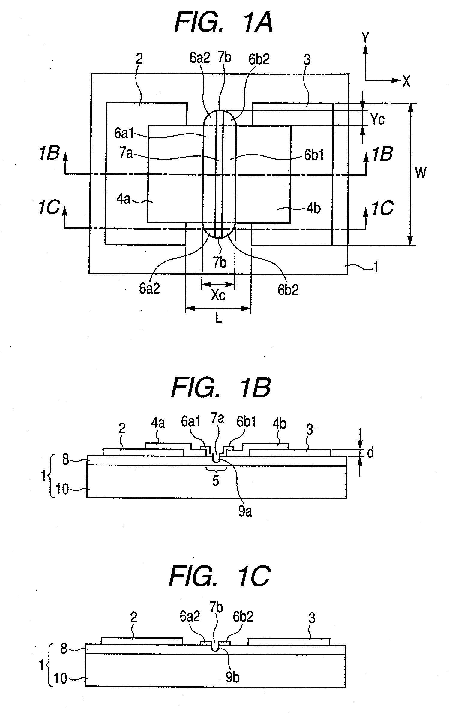
[0100]The electron-emitting device illustrated in FIGS. 1A to 1C was manufactured through the steps illustrated in FIGS. 2A to 2E.
[0101](Step-a)
[0102]The glass base material 10 (produced by Asahi Glass Co. Ltd., PD200) was sufficiently cleaned with a cleaning solution, deionized water, and an organic solvent. Then, the passivation layer 8 made of SiO2 was deposited on the base material 10 at a thickness of approximately 250 nm using an Rf sputtering apparatus, to prepare the substrate 1 (FIG. 2A).
[0103](Step-b)
[0104]A Ti layer having a thickness of 5 nm and a Pt layer having a thickness of 40 nm were successively deposited on the substrate 1 by a sputtering process. Then, an etching mask (photoresist) was formed so as to cover a pattern of the first and second electrodes 2 and 3. Next, dry etching using Ar plasma was performed and subsequently a remaining portion of the etching mask was removed by dissolving to form the first and second electrodes 2 and 3 (FIG. 2B). The interval L b...
example 2
[0128]An electron-emitting device manufactured in this example is different from Example 1 in that the passivation layer 8 is not used. Hereinafter, a method of manufacturing the electron-emitting device according to this example is described step by step with reference to FIGS. 2A to 2E.
[0129](Step-a)
[0130]A quartz glass substrate was sufficiently cleaned with deionized water and an organic solvent to prepare the substrate 1.
[0131]Step-b to Step-d were performed in the same manner as in Example 1.
[0132]Step-e and Step-f were performed in the same manner as in Example 1, except that the peak was adjusted to ±15 V.
[0133]After the steps, an observation using an optical microscope was performed. As a result, it was determined that the electron-emitting device having the structure schematically illustrated in FIG. 1A was obtained. In the first and second extending portions 6a2 and 6b2, Xc of FIG. 1A was 9.2 μm and Yc of FIG. 1A was 3.2 μm.
[0134]The first and second extending portions 6a...
example 3
[0142]FIG. 9 is an explanatory view illustrating an electron-emitting device according to this example.
[0143]The electron-emitting device according to this example is different from that of Example 1 in that the conductive film 4 of the electron-emitting device according to Example 1 was formed by an ink-jet process and the passivation layer 8 was formed using a polysilazane solution. Others are fundamentally performed in the same manner as in Example 1.
[0144]Hereinafter, a method of manufacturing the electron-emitting device according to this example is described step by step with reference to FIG. 9 and FIGS. 2A to 2E.
[0145](Step-a)
[0146]A glass substrate made of soda lime glass was sufficiently cleaned with a cleaning solution, deionized water, and an organic solvent. The polysilazane solution, Aquamica (produced by AZ Electronic Materials, NN110-20) was spin-applied onto the glass substrate for 30 seconds at 2,000 revolutions / minute. Subsequently, the glass substrate was dried a...
PUM
 Abstract
Description
Claims
Application Information
 - R&D
- Intellectual Property
- Life Sciences
- Materials
- Tech Scout
- Unparalleled Data Quality
- Higher Quality Content
- 60% Fewer Hallucinations
Browse by: Latest US Patents, China's latest patents, Technical Efficacy Thesaurus, Application Domain, Technology Topic, Popular Technical Reports.
© 2025 PatSnap. All rights reserved.Legal|Privacy policy|Modern Slavery Act Transparency Statement|Sitemap|About US| Contact US: help@patsnap.com


