Low-cost substrates having high-resistivity properties and methods for their manufacture
- Summary
- Abstract
- Description
- Claims
- Application Information
AI Technical Summary
Benefits of technology
Problems solved by technology
Method used
Image
Examples
Embodiment Construction
[0015]The preferred embodiments and particular examples described herein should be seen as examples of the scope of the invention, but not as limiting the present invention. The scope of the present invention should be determined with reference to the claims.
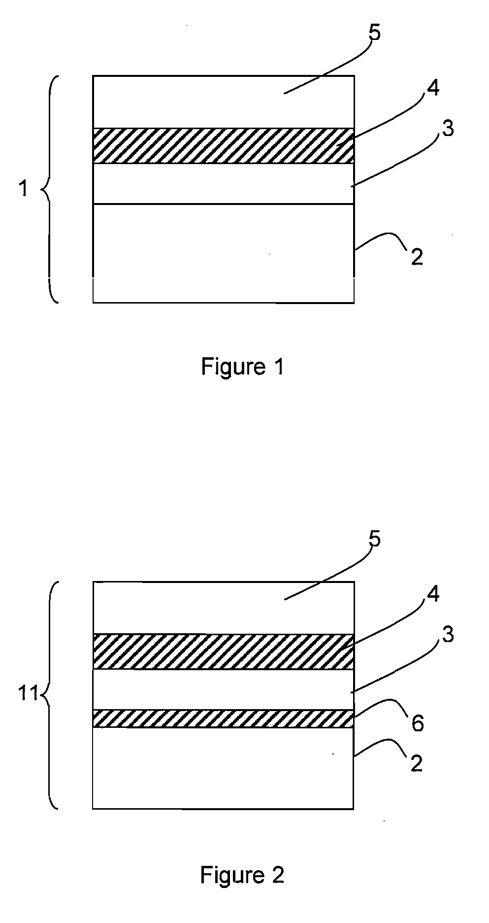
[0016]FIG. 1 illustrates embodiments according to the invention of substrates 1 structured so that devices fabricated in a top layer thereof have properties similar to the same devices fabricated in a standard high resistivity substrate. These substrates of the invention are also more simply referred to herein as “HR substrates”. The substrate 1 can have a diameter depending on its final application of, e.g., 300 mm, 200 mm, or other diameters.
[0017]Substrate 1 comprises top layer 5, in which or on which devices are ultimately formed. In some cases, devices, e.g., known CMOS devices, can be formed according to known techniques directly on and in top layer 5. In other cases, e.g., gallium nitride HEMT devices, further layers (not...
PUM
 Abstract
Description
Claims
Application Information
 - R&D
- Intellectual Property
- Life Sciences
- Materials
- Tech Scout
- Unparalleled Data Quality
- Higher Quality Content
- 60% Fewer Hallucinations
Browse by: Latest US Patents, China's latest patents, Technical Efficacy Thesaurus, Application Domain, Technology Topic, Popular Technical Reports.
© 2025 PatSnap. All rights reserved.Legal|Privacy policy|Modern Slavery Act Transparency Statement|Sitemap|About US| Contact US: help@patsnap.com


