Manufacturing method of optical waveguide device
a manufacturing method and waveguide technology, applied in the field of fabrication methods of optical waveguide devices, can solve the problems of diffuse reflection, increased propagation loss of light propagating inside the core,
- Summary
- Abstract
- Description
- Claims
- Application Information
AI Technical Summary
Benefits of technology
Problems solved by technology
Method used
Image

Examples
examples
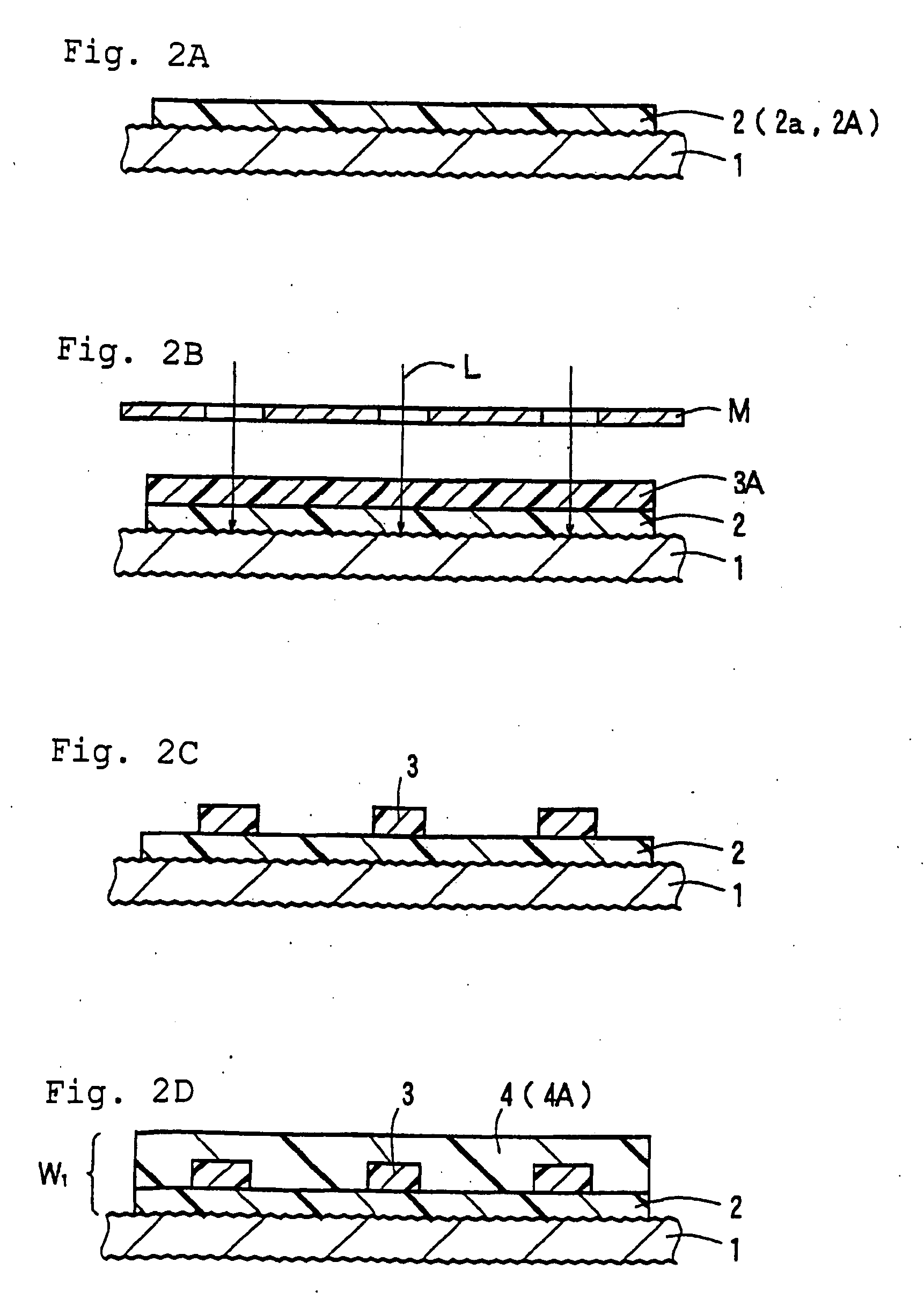
Metal Substrate
[0044]SUS 304 foil [manufactured by Toyo Seihaku Co., Ltd., and having a thickness of 20 μm and an arithmetic mean roughness (Ra) of 0.8 μm] was prepared.
Material for Formation of Under Cladding Layer and Over Cladding Layer
[0045]A material for formation of an under cladding layer and an over cladding layer was prepared by mixing 35 parts by weight of bisphenoxyethanol fluorene glycidyl ether (component A) represented by the following general formula (1), 40 parts by weight of 3′,4′-epoxycyclohexyl methyl-3,4-epoxycyclohexane carboxylate which was an alicyclic epoxy resin (CELLOXIDE 2021P manufactured by Daicel Chemical Industries, Ltd.) (component B), 25 parts by weight of (314′-epoxycyclohexane)methyl-3′,4′-epoxycyclohexyl-carboxylate (CELLOXIDE 2081 manufactured by Daicel Chemical Industries, Ltd.) (component C), and 2 parts by weight of a 50% propione carbonate solution of 4,4′-bis[di(β-hydroxyethoxy)phenylsulfinio]phenyl-sulfide-bis-hexafluoroantimonate (componen...
PUM
| Property | Measurement | Unit |
|---|---|---|
| Ra | aaaaa | aaaaa |
| thickness | aaaaa | aaaaa |
| thickness | aaaaa | aaaaa |
Abstract
Description
Claims
Application Information
 - Generate Ideas
- Intellectual Property
- Life Sciences
- Materials
- Tech Scout
- Unparalleled Data Quality
- Higher Quality Content
- 60% Fewer Hallucinations
Browse by: Latest US Patents, China's latest patents, Technical Efficacy Thesaurus, Application Domain, Technology Topic, Popular Technical Reports.
© 2025 PatSnap. All rights reserved.Legal|Privacy policy|Modern Slavery Act Transparency Statement|Sitemap|About US| Contact US: help@patsnap.com