
Process for Producing Siliceous Film and Substrate With The Siliceous Film Produced by The Process

a technology of process and siliceous film, which is applied in the direction of coatings, chemical vapor deposition coatings, semiconductor devices, etc., can solve the problems of difficult formation of fine isolation structures suitable for a necessary level of integration, voids formed in grooves, and deterioration of physical strength and insulating properties of the substrate, etc., to achieve excellent mechanical strength, no deterioration in properties, and even etching rate

Inactive Publication Date: 2009-11-12
ISHIKAWA TOMONORI +1
View PDF3 Cites 6 Cited by
  • Summary
  • Abstract
  • Description
  • Claims
  • Application Information

AI Technical Summary

Benefits of technology

"The present invention provides a process for producing a siliceous film that can be used in electronic devices such as semiconductor devices. The process involves forming an insulating film with a hydrogen content of not less than 9×10²⁰ atms / cm3 as measured by a secondary ion mass spectrometry on a surface of a silicon substrate having concavoconvexes, coating a composition containing a polysilazane compound on the substrate, and heating the coated substrate to convert the polysilazane compound to a silicon dioxide film. The resulting siliceous film has a homogeneous quality over its entire part and is useful for realizing a higher level of integration in electronic devices."

Problems solved by technology

The progress of an increase in density and an enhancement in level of integration makes it difficult to form a fine isolation structure suitable for a necessary level of integration.
According to this method, however, when the inside of fine grooves, for example, having a size of not more than 100 nm which has recently been demanded, is filled, in some cases, voids were formed within the grooves.
These structure defects are causative of a deterioration in physical strength and insulating properties of the substrate.
This method, however, is disadvantageous in that, in converting silicon hydroxide to silicon dioxide, volume shrinkage occurs resulting in cracking.
According to studies conducted by the present inventor, however, it was found that, in this trench isolation structure, in the conversion of polysilazane to silicon dioxide to form a siliceous film, there is a slight difference in reaction conditions between the surface part of the coating film and the inside of the trench, and, thus, the quality of the siliceous film in the inside of the trench is different from the quality of the siliceous film on the outside of the trench, or the quality of the siliceous film varies depending upon the depth within the groove, posing a problem that the etching rate is uneven.
This problem is significant when low-temperature treatment, which is required due to a restriction of device design and process design, is carried out.

Method used


Image

  • Process for Producing Siliceous Film and Substrate With The Siliceous Film Produced by The Process
  • Process for Producing Siliceous Film and Substrate With The Siliceous Film Produced by The Process
  • Process for Producing Siliceous Film and Substrate With The Siliceous Film Produced by The Process

Examples


example 1

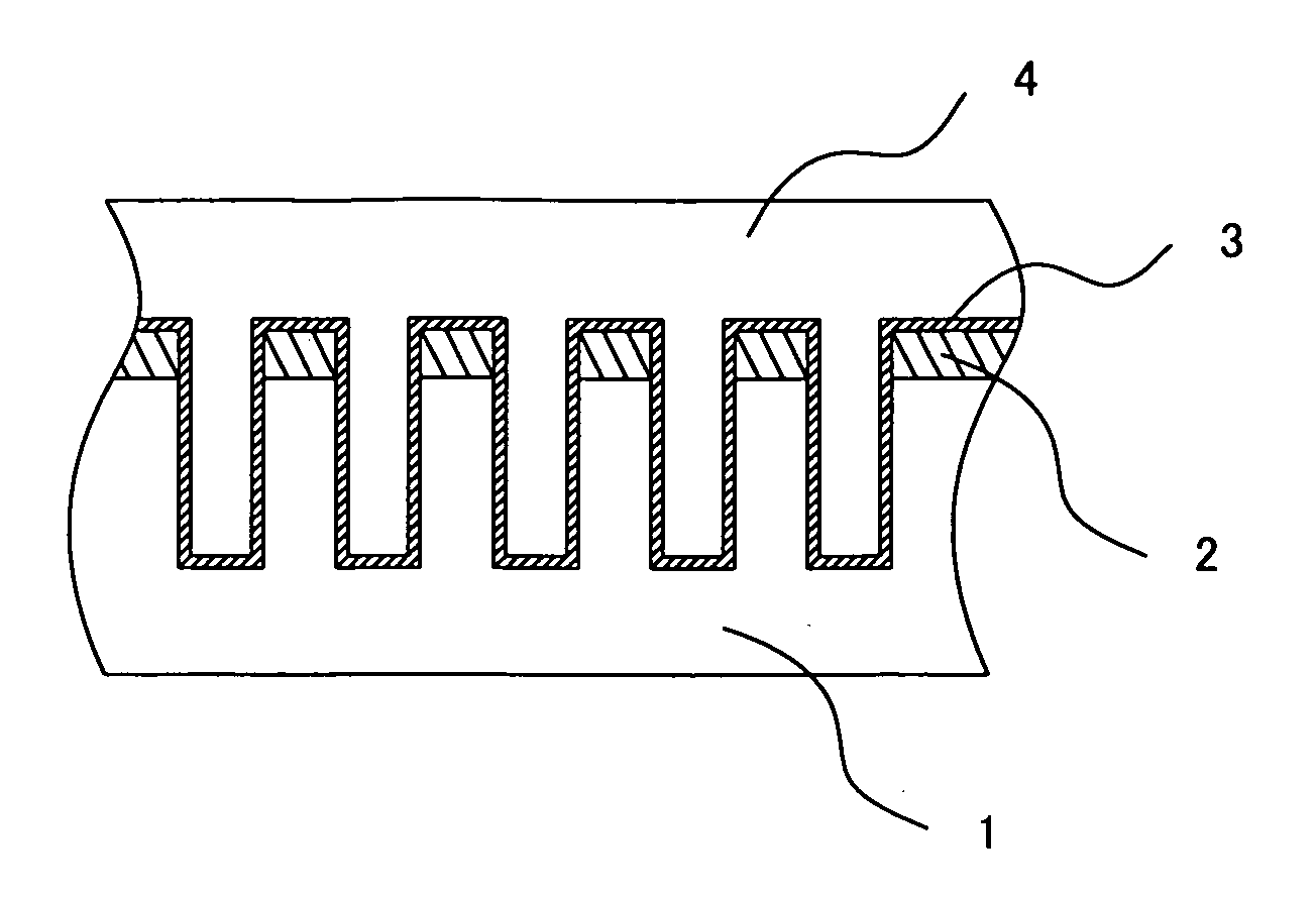
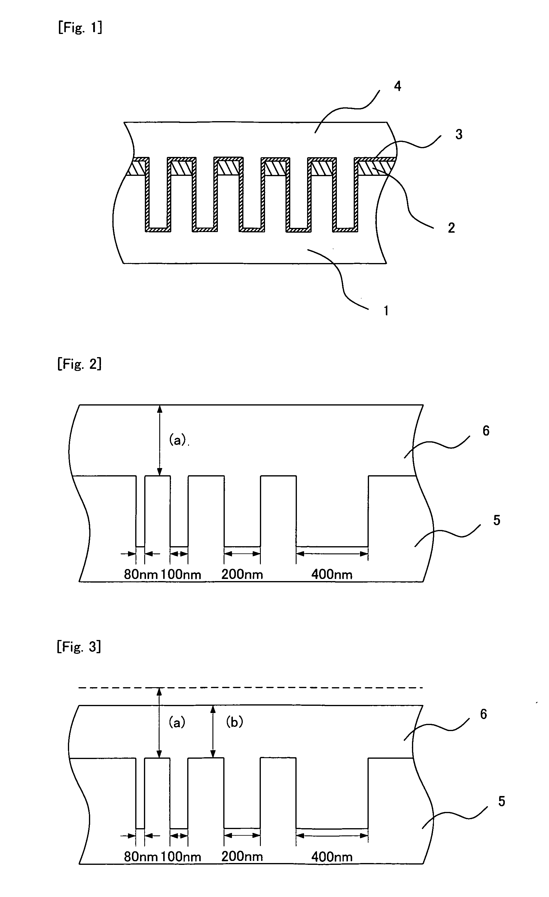
[0078]The present invention will be further described with reference to the following Example which illustrate a contemplated technique for embedding element isolation grooves of STI (shallow trench isolation) structures in conjunction with FIG. 1.

[0079]A grooved sample for the evaluation of a construction as shown in FIG. 1 was first provided. This grooved sample has been formed by depositing a silicon nitride (SiN) film 2 on an upper surface of a silicon substrate 1, for example, to a thickness of 150 nm and then forming grooves by lithography and dry etching (five grooves are shown in the drawing). In this case, for all the five grooves, the width was, for example, 80 nm to 400 nm, and the depth was, for example, 450 nm (the depth of the silicon substrate part was 300 nm).

[0080]A 20 nm-thick silicon dioxide film 3 was deposited on the grooved sample having the above construction by plasma chemical vapor deposition (plasma TEOS) using TEOS as a silicon source.

[0081]The silicon dio...

example 2

[0087]A sample was prepared in the same manner as in Example 1, except that a 20 nm-thick silicon nitride film was deposited instead of the plasma TEOS film shown in FIG. 1 by plasma chemical vapor deposition (PE-CVD). The silicon nitride film 3 was formed by the above PE-CVD under the following film forming conditions. SiH4 / NH3 gas flow rate and source power / bias power: SiH4 / NH3=55 / 110 sccm, SRF / BRF=4400 / 2600 W, and substrate temperature=400° C.

[0088]SIMS analysis and TDS measurement have revealed that the plasma PE-CVD film contained an excessive amount of hydrogen. Specifically, according to the SIMS analysis, the content of hydrogen in the film was about 1×10²¹ atms / cm3, and, according to the TDS analysis, it was confirmed that hydrogen was released from the film in vacuo at a temperature around 350° C., indicating that this film contained hydrogen.

[0089]The film formation using the polysilazane solution and the heat treatment were carried out in the same manner as in Example 1....

example 3

[0097]A sample was prepared in the same manner as in Example 1, except that a 20 nm-thick silicon dioxide film was deposited instead of the plasma TEOS film shown in Example 1 by plasma chemical vapor deposition using SiH4 and O2 as a source.

[0098]The silicon dioxide film 3 was formed under the following film forming conditions. SiH4 / O2 gas flow rate and source power / bias power: SiH4 / O2=50 / 100 sccm, SRF / BRF=4500 / 3000 W, and substrate temperature=250° C.

[0099]SIMS analysis and TDS measurement have revealed that the silicon dioxide film contained an excessive amount of hydrogen. Specifically, according to the SIMS analysis, the content of hydrogen in the film was about 1.5×10²¹ atms / cm3.

[0100]The film formation using the polysilazane solution and the heat treatment were carried out in the same manner as in Example 1.


PUM

PropertyMeasurementUnit
thicknessaaaaaaaaaa
sizeaaaaaaaaaa
thicknessaaaaaaaaaa

Abstract

An objective of the present invention is to provide a process for producing a siliceous film which has a uniform quality independently of sites and in both the inside and outside of the grooves and is free from voids and cracks in the inside of the grooves. A substrate with the siliceous film can be produced by forming an insulating film having a high hydrogen content on a surface of a silicon substrate having concavoconvexes, then coating a composition containing a polysilazane compound on the substrate, and heating the coated substrate to convert the polysilazane compound to a silicon dioxide film.

Description

TECHNICAL FIELD[0001]This invention relates to a process for producing a siliceous film for use in electronic devices, and a substrate with the siliceous film produced by the process. The present invention also relates to a method for forming a shallow trench isolation structure formed for insulating an electronic device using a polysilazane compound in the production of electronic devices such as semiconductor elements.BACKGROUND ART[0002]In general, in electronic devices such as semiconductor devices, semiconductor elements, for example, transistors, resistors and the like are disposed on a substrate. These should be electrically insulated. Accordingly, a region for element isolation should be provided between the elements. This region is called an isolation region. In general, this isolation region has hitherto been provided by selectively forming an insulating film on a surface of a semiconductor substrate.[0003]On the other hand, in the field of electronic devices, increased de...

Claims


Application Information

Patent Timeline
Patent Type & Authority Applications(United States)
IPC IPC(8): H01L29/06H01L21/316H01L21/762
CPCC23C16/56H01L21/02164H01L21/02222H01L21/02282H01L21/76227H01L21/02337H01L21/3125H01L21/316H01L21/02304H01L21/02326H01L21/76C23C16/40
Inventor ISHIKAWA, TOMONORITERUNO
Owner ISHIKAWA TOMONORI
Learn More