
Fully-depleted low-body doping field effect transistor (FET) with reverse short channel effects (SCE) induced by self-aligned edge back-gate(s)

a low-body, doping field effect transistor technology, applied in the direction of semiconductor devices, electrical equipment, basic electric elements, etc., can solve the problems of increased off-state leakage current between the source and drain region, performance limitations referred to as short-channel effects, etc., to avoid cross-chip threshold voltage variation and minimize off-state leakage current

Inactive Publication Date: 2009-10-22
GLOBALFOUNDRIES INC
View PDF50 Cites 3 Cited by
  • Summary
  • Abstract
  • Description
  • Claims
  • Application Information

AI Technical Summary

Benefits of technology

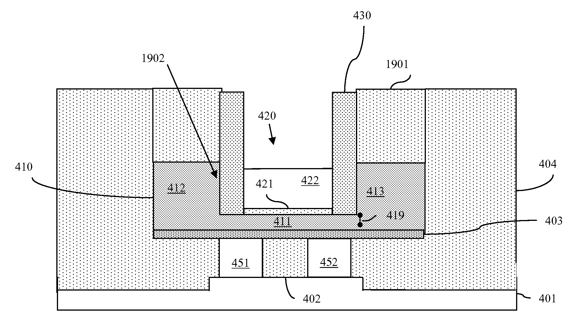
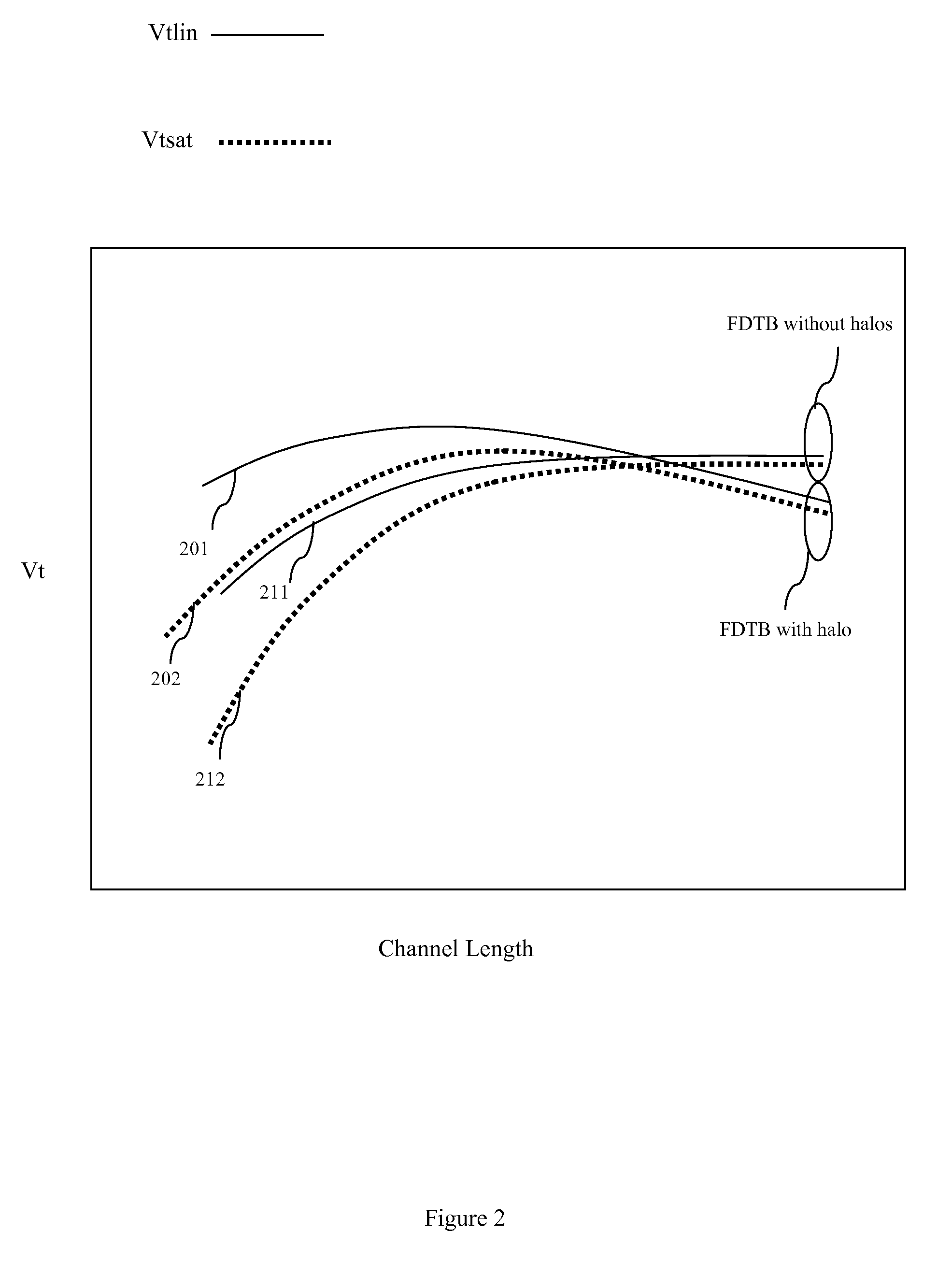
[0005]In view of the foregoing, disclosed herein are embodiments of a field effect transistor (FET) and, more particularly, a fully-depleted, thin-body (FDTB) FET that allows for scaling with minimal short channel effects, such as drain induced barrier lowering (DIBL) and saturation threshold voltage (Vtsat) roll-off, at shorter channel lengths. The FDTB FET embodiment are configured with either an edge back-gate or split back-gate that can be biased in order to selectively adjust the potential barrier between the source / drain regions and the channel region for minimizing off-state leakage current between the drain region and the source region and / or for varying threshold voltage. These unique back-gate structures avoid the need for halo doping to ensure linear threshold voltage (Vtlin) roll-up at smaller channel lengths and, thus, avoid across-chip threshold voltage variations due to random doping fluctuations. Also disclosed are method embodiments for forming such FETs.
[0008]A first insulator layer can be positioned adjacent to the edge back-gate on one side such that it is below the center of the channel region and further extends below the interface between the channel region and the drain region to below the drain region. A second insulator layer can be positioned adjacent the edge back-gate on the opposite side such that it is below the end of the source region. The width of the edge back-gate can be predetermined such that it is at least equal to the thickness of the semiconductor layer in the channel region. In operation, the edge back-gate can be electrically connected to a supply voltage and can be biased in order to selectively adjust a potential barrier between the source region and the channel region for minimizing off-state leakage current between the drain region the source region and / or for varying threshold voltage.
[0011]A first insulator layer can fill the gap between the two sections of the split back-gate and below the center of the channel region. A second insulator layer can be positioned adjacent the outer sidewalls of the split back-gate below the source / drain regions. As with the previously described embodiment, in operation, one or both of the discrete sections of the split back-gate can be electrically connected to a supply voltage and can be biased in order to selectively adjust a potential barrier between the source / drain regions and the channel region for minimizing off-state leakage current between the source / drain regions and / or for varying threshold voltage.
[0016]In operation, the edge back-gate of this FDTB FET can be electrically connected to a supply voltage (e.g., Vdd or ground) and can be biased in order to selectively adjust the potential barrier between the source region and the channel region for minimizing off-state leakage current between the drain region and the source region and / or for varying threshold voltage.
[0022]In operation, the discrete portions of the split back-gate can be electrically connected to a supply voltage and can be biased in order to selectively adjust the potential barrier between the source / drain regions and the channel region for minimizing off-state leakage current between the drain region and the source region and / or for varying threshold voltage.

Problems solved by technology

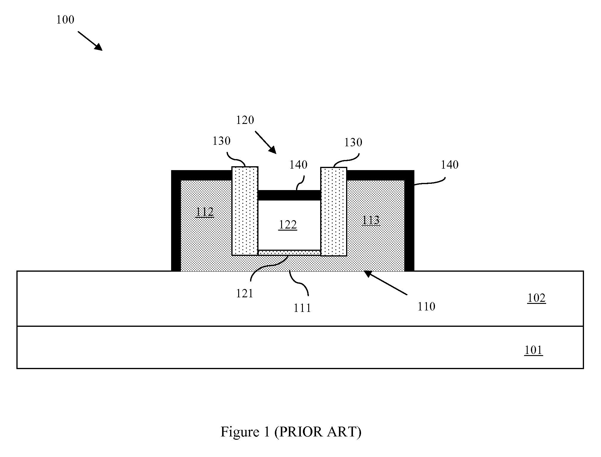
As field effect transistor (FET) size continues to be scaled and, more particularly, as channel length is reduced, performance limitations referred to as “short-channel effects” arise.
DIBL and Vtsat roll-off can both result in an increased off-state leakage current between the source and drain regions.

Method used


Image

  • Fully-depleted low-body doping field effect transistor (FET) with reverse short channel effects (SCE) induced by self-aligned edge back-gate(s)
  • Fully-depleted low-body doping field effect transistor (FET) with reverse short channel effects (SCE) induced by self-aligned edge back-gate(s)
  • Fully-depleted low-body doping field effect transistor (FET) with reverse short channel effects (SCE) induced by self-aligned edge back-gate(s)

Examples


Embodiment Construction

[0046]The embodiments of the invention and the various features and advantageous details thereof are explained more fully with reference to the non-limiting embodiments that are illustrated in the accompanying drawings and detailed in the following description. It should be noted that the features illustrated in the drawings are not necessarily drawn to scale. Descriptions of well-known components and processing techniques are omitted so as to not unnecessarily obscure the embodiments of the invention. The examples used herein are intended merely to facilitate an understanding of ways in which the embodiments of the invention may be practiced and to further enable those of skill in the art to practice the embodiments of the invention. Accordingly, the examples should not be construed as limiting the scope of the embodiments of the invention.

[0047]As mentioned above, as field effect transistor (FET) size continues to be scaled and, more particularly, as channel length is reduced, per...


PUM


Abstract

Disclosed are embodiments of a field effect transistor (FET) and, more particularly, a fully-depleted, thin-body (FDTB) FET that allows for scaling with minimal short channel effects, such as drain induced barrier lowering (DIBL) and saturation threshold voltage (Vtsat) roll-off, at shorter channel lengths. The FDTB FET embodiments are configured with either an edge back-gate or split back-gate that can be biased in order to selectively adjust the potential barrier between the source / drain regions and the channel region for minimizing off-state leakage current between the drain region and the source region and / or for varying threshold voltage. These unique back-gate structures avoid the need for halo doping to ensure linear threshold voltage (Vtlin) roll-up at smaller channel lengths and, thus, avoid across-chip threshold voltage variations due to random doping fluctuations. Also disclosed are method embodiments for forming such FETs.

Description

BACKGROUND[0001]1. Field of the Invention[0002]The embodiments of the invention generally relate to fully-depleted, thin-body, field effect transistors and, more particularly, to a fully-depleted, thin-body, field effect transistor that exhibits relatively small drain-induced barrier lowering without requiring body doping or halos.[0003]2. Description of the Related Art[0004]As field effect transistor (FET) size continues to be scaled and, more particularly, as channel length is reduced, performance limitations referred to as “short-channel effects” arise. Such short-channel effects include, but art not limited to, drain-induced barrier lowering (DIBL) and saturation threshold voltage (Vtsat) roll-off. Specifically, DIBL refers to the fact that in a FET with a relatively short channel length the potential barrier that exists between the drain region and the source region is reduced by the electrostatic influence of the drain voltage. Vtsat roll-off refers to the fact that the relati...

Claims


Application Information

Patent Timeline
Patent Type & Authority Applications(United States)
IPC IPC(8): H01L49/00H01L21/00H10N99/00
CPCH01L29/66621H01L29/78603H01L29/78696H01L29/78648H01L29/78645
Inventor ADKISSON, JAMES W.ANDERSON, BRENT A.BRYANT, ANDRESCLARK, JR., WILLIAM F.NOWAK, EDWARD J.
Owner GLOBALFOUNDRIES INC
Learn More