
Method for Manufacturing Epitaxial Wafer and Epitaxial Wafer

a manufacturing method and technology for epitaxial wafers, applied in the direction of crystal growth process, synthetic resin layered products, silicon compounds, etc., can solve the problems of significantly degrading productivity or yield ratio, and affecting the quality of epitaxial wafers. achieve the effect of high flatness degr

Inactive Publication Date: 2009-10-08
SHIN-ETSU HANDOTAI CO LTD
View PDF5 Cites 12 Cited by
  • Summary
  • Abstract
  • Description
  • Claims
  • Application Information

AI Technical Summary

Benefits of technology

[0012]In view of the above-explained problem, it is an object of the present invention to provide a method that enables manufacturing an epitaxial wafer having a small roll-off value by controlling a thickness of an epitaxial layer near the outermost periphery at the time of epitaxial growth.

Problems solved by technology

However, in shape measurement based on these methods, an outer peripheral shape outside from an edge of a wafer than 3 mm cannot be accurately measured because of limitations in principle and structure of an apparatus.
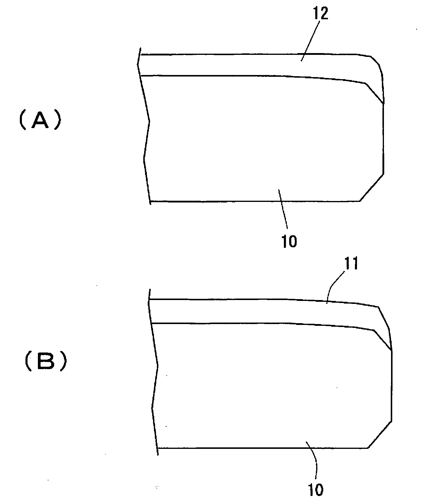
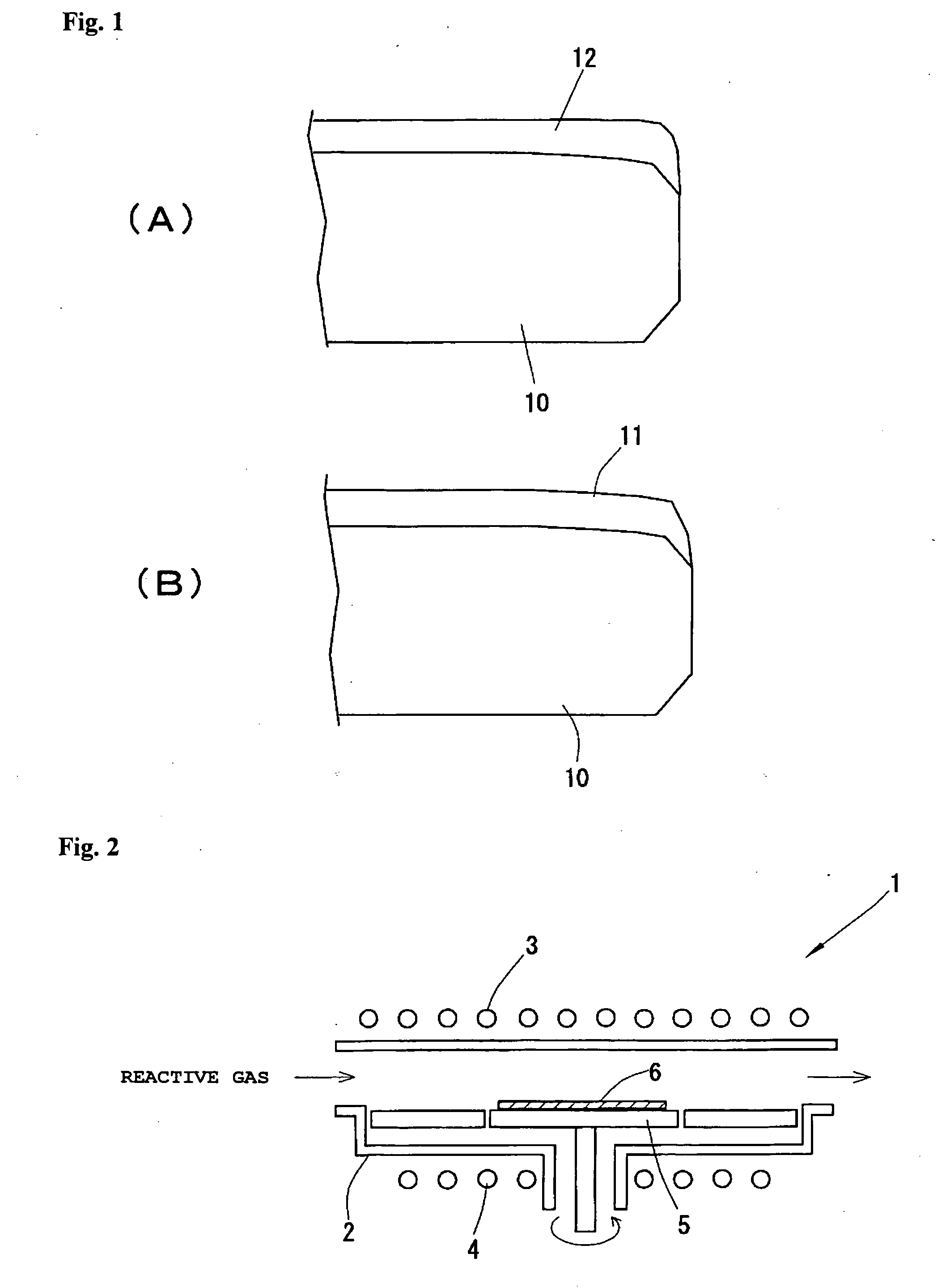
10, and there is a problem that a roll-off is degraded due to an epitaxial growth process as compared with that of a silicon wafer 10 before epitaxial growth.
However, this method has a problem that particle generation or cracks may possibly occur due to diameter reduction chamfering or fusion cutting after epitaxial growth and a wafer becomes small in size because the wafer is subjected to diameter reduction or fusion cutting after epitaxial growth, thereby substantially considerably degrading productivity or a yield ratio.

Method used


Image

  • Method for Manufacturing Epitaxial Wafer and Epitaxial Wafer
  • Method for Manufacturing Epitaxial Wafer and Epitaxial Wafer
  • Method for Manufacturing Epitaxial Wafer and Epitaxial Wafer

Examples


example

[0057]A silicon wafer having a diameter of 300 mm was prepared, and DynaSearch (manufactured by Raytex Corporation) was used as a flatness / nanotopography measurement apparatus to measure a height displacement amount of a surface at a wafer peripheral portion, and a measured value was determined as a roll-off amount.

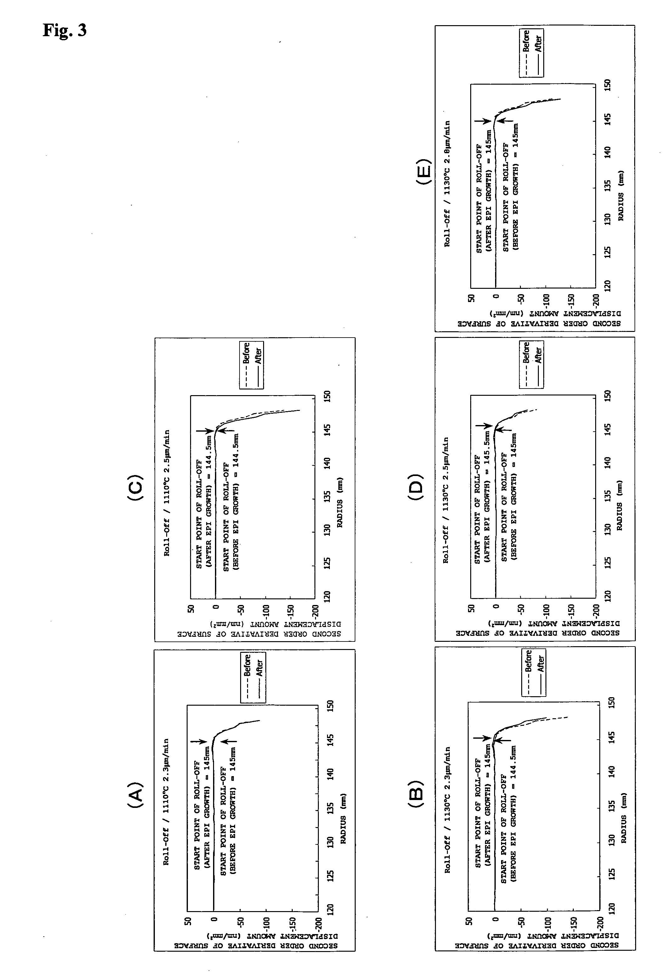
[0058]In order to compensate a sagging shape of the peripheral portion when performing epitaxial growth with respect to this wafer, a growth temperature was set to 1130° C. and a growth rate was set to 2.5 μm / min based on the correlations depicted in FIGS. 5 and 6 to perform epitaxial growth. Further, a surface displacement amount of the manufactured epitaxial wafer was measured like the silicon wafer before epitaxial growth.

[0059]FIG. 11 shows surface displacement amounts of the silicon wafer and the epitaxial wafer, in which an ordinate represents a value of a second order derivative of the surface displacement amount and an abscissa represents a distance (a radius) fro...


PUM

PropertyMeasurementUnit
diameteraaaaaaaaaa
thicknessaaaaaaaaaa
radiusaaaaaaaaaa

Abstract

The present invention provides a method for manufacturing an epitaxial wafer by supplying a raw material gas onto a silicon wafer to perform vapor-phase growth of an epitaxial layer, wherein a thickness of the epitaxial layer that is formed at a peripheral portion of the silicon wafer is controlled by controlling a growth rate and / or a growth temperature of the epitaxial layer that is subjected to vapor-phase growth. As a result, there is provided the method that enables manufacturing an epitaxial wafer having a small roll-off value by controlling a thickness of an epitaxial layer near the outermost periphery at the time of epitaxial growth.

Description

TECHNICAL FIELD[0001]The present invention relates to a method for manufacturing an epitaxial wafer and an epitaxial wafer.BACKGROUND ART[0002]When fabricating a semiconductor device, an epitaxial wafer having an epitaxial layer formed on a silicon wafer may be used in some cases. The epitaxial wafer can be generally manufactured by introducing a raw material gas (e.g., SiCl4 or SiHCl3) into a reactor and growing a silicon single crystal layer (an epitaxial layer) on a silicon single crystal wafer heated to a high temperature.[0003]Film thickness uniformity of the epitaxial layer is one of the most important quality items of the epitaxial wafer, and generally evaluated by an optical measurement method using an infrared ray. Further, a thickness uniformity (flatness) of the entire epitaxial wafer is evaluated by a technique using an electric capacitance or an optical displacement gauge as a fundamental principle.[0004]However, in shape measurement based on these methods, an outer per...

Claims


Application Information

Patent Timeline
Patent Type & Authority Applications(United States)
IPC IPC(8): B32B5/00C30B25/16C01B33/02
CPCC30B25/02C30B25/16C30B25/165H01L21/02634H01L21/02381H01L21/02532H01L21/0262C30B29/06C23C16/24
Inventor KANAYA, KOICHIOHNISHI, MASATO
Owner SHIN-ETSU HANDOTAI CO LTD
Learn More