Chemical mechanical polishing method and method of manufacturing semiconductor device
a technology of mechanical polishing and semiconductor devices, which is applied in the direction of manufacturing tools, lapping machines, other chemical processes, etc., can solve the problem of not being able to achieve the flatness of the first organic film b>9/b>, and achieve the effect of reducing the resistance of metal interconnects and wire-to-wire capacitance, reducing the number of steps, and increasing yield
- Summary
- Abstract
- Description
- Claims
- Application Information
AI Technical Summary
Benefits of technology
Problems solved by technology
Method used
Image
Examples
example 1
2-1. Example 1
[0133]This example illustrates a hybrid dual damascene processing method by a dual hard mask method using an ArF excimer laser incorporating planarization of an organic film by CMP.
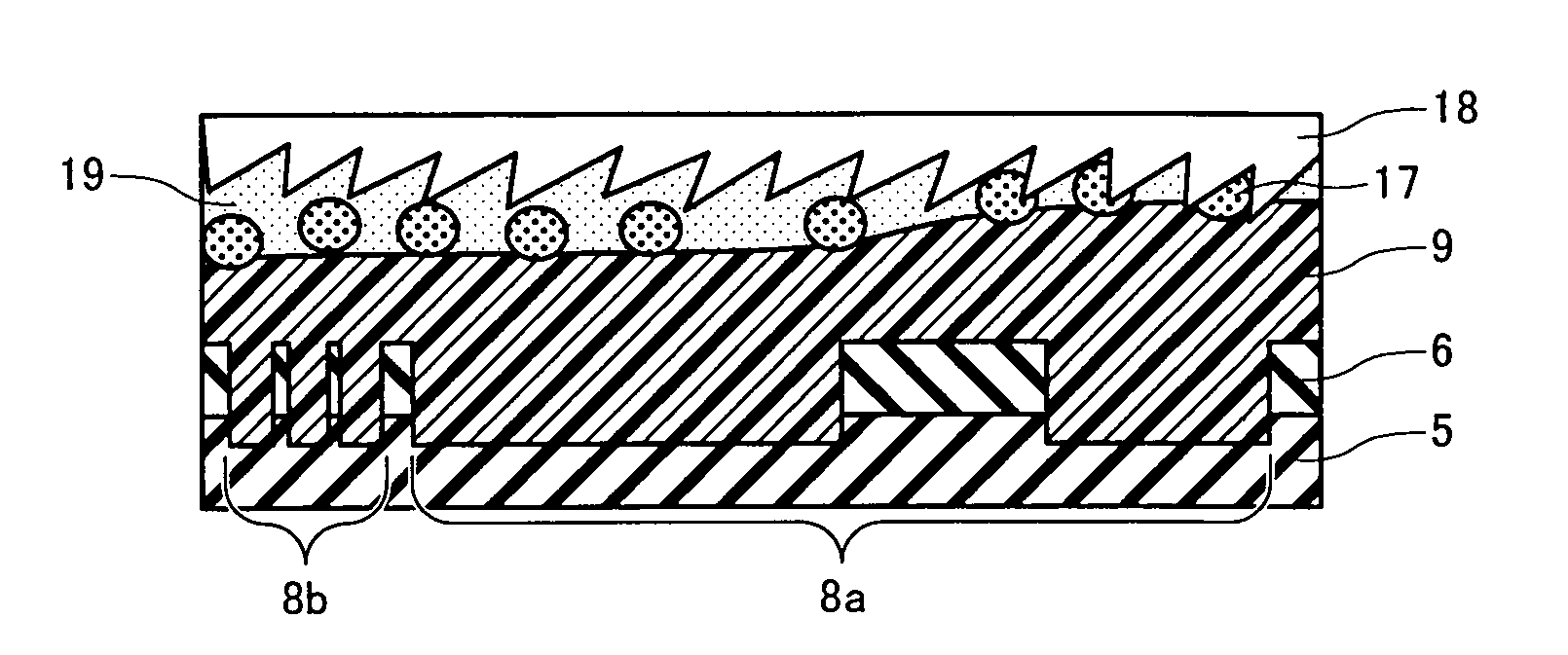
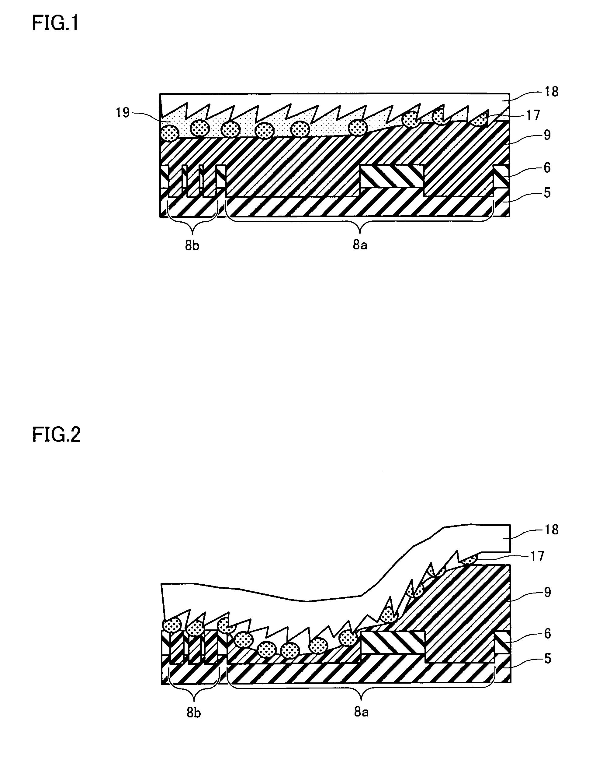
[0134]This example illustrates the case of chemical mechanical polishing the first organic film 9 using the above slurry 1.
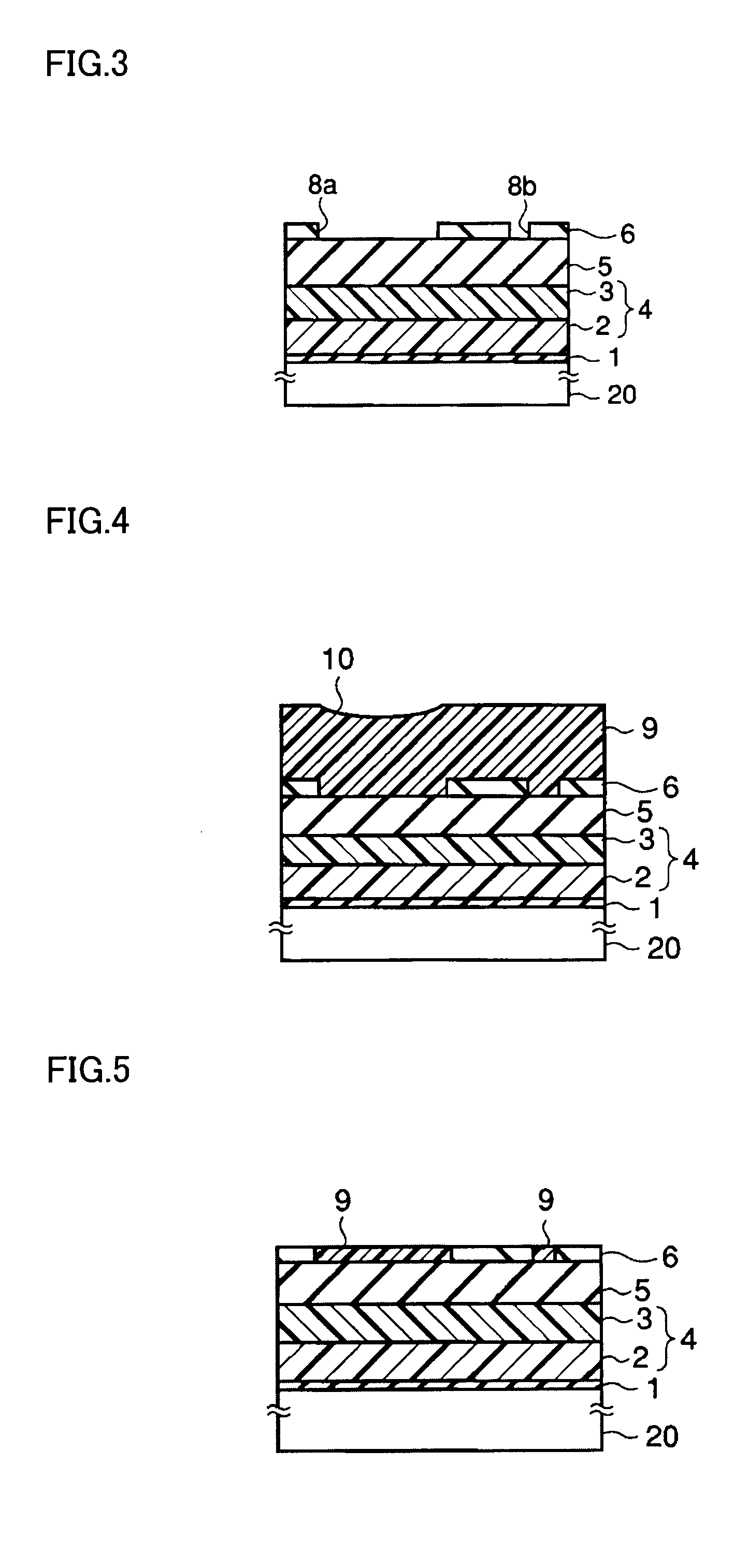
[0135]As shown in FIG. 3, an organic insulating film 4 and the first and second hard masks 5 and 6 including an inorganic material were formed in that order on a semiconductor substrate 20 on which an element (not shown) was formed. The interconnect groove patterns 8a and 8b as depressions were formed in the second hard mask 6. In the example shown in FIG. 3, the organic insulating film 4 has a two-layer structure formed of a first organic insulating film 2 and a second organic insulating film 3. An etching stopper film 1 is formed in the lower layer of these films.
[0136]An interlayer dielectric (not shown) in which a first interconnect layer is formed is provided betwee...
example 2
2-3. Example 2
[0167]In this example, hybrid dual damascene processing by a dual hard mask method using an ArF excimer laser incorporating planarization of an organic film by CMP was performed in the same manner as in Example 1.
[0168]In this example, the first organic film 9 was chemically and mechanically polished using the above slurry 3.
[0169]In more detail, the interconnect groove patterns 8a and 8b were formed in the second hard mask 6 (SiN film) using the method described in Example 1. The first organic film 9 was formed by coating and planarized by CMP.
[0170]In this example, the first organic film 9 was planarized using the device, polishing pad, load, and rotational speed described in Example 1 except for using the slurry 3 as the CMP slurry. Specifically, a slurry (slurry 3) was used which was produced by mixing crosslinked PST particles (crosslinked polymer particles) (abrasive) with an average particle diameter of 50 nm, which was smaller than that of the polymer particles...
example 3
2-10. Example 3
[0193]In this example, hybrid dual damascene processing was performed by a dual hard mask method using an ArF excimer laser incorporating planarization of an organic film by CMP.
[0194]In Example 1, two organic films were used as the lower-layer film 12. In Example 1, the resist containing a novolac resin as the main component (IX370G manufactured by JSR Corporation) was applied to form the first organic film 9. After planarizing the first organic film 9 by CMP, CT01 was applied to form the second organic film 11. This aims at improving the lithographic performance by using IX370G (first organic film 9) which exhibits excellent embedding characteristics and planarization characteristics and CT01 (second organic film 11) which can function as the anti-reflective film during lithography using an ArF excimer laser in combination.
[0195]In this example, the organic film 9 containing a novolac resin as the main component (ODL-50 manufactured by JSR Corporation) was used as t...
PUM
| Property | Measurement | Unit |
|---|---|---|
| zeta potential | aaaaa | aaaaa |
| particle diameter | aaaaa | aaaaa |
| particle diameter | aaaaa | aaaaa |
Abstract
Description
Claims
Application Information
 - R&D
- Intellectual Property
- Life Sciences
- Materials
- Tech Scout
- Unparalleled Data Quality
- Higher Quality Content
- 60% Fewer Hallucinations
Browse by: Latest US Patents, China's latest patents, Technical Efficacy Thesaurus, Application Domain, Technology Topic, Popular Technical Reports.
© 2025 PatSnap. All rights reserved.Legal|Privacy policy|Modern Slavery Act Transparency Statement|Sitemap|About US| Contact US: help@patsnap.com


