Solid-state image pickup device

Inactive Publication Date: 2009-09-17
CANON KK
View PDF15 Cites 20 Cited by
  • Summary
  • Abstract
  • Description
  • Claims
  • Application Information

AI Technical Summary

Benefits of technology

[0023]In light of the above, the present invention provides a solid-state image pickup device in which horizontal noise is reduced.

Problems solved by technology

In this configuration, image quality may be deteriorated because of noise generated by a mechanism described below.
This increases the noise in the several thousand kilohertz band.
Considering the current consumption, the number of transistors 604a to be connected in parallel cannot be increased easily.
This means that, if a change in the potential of the voltage supply wire changes the level of a signal that is processed by the signal-processing circuit, there is a possibility that a mechanism similar to the one described above causes horizontal noise.
For example, in a case of an amplifier circuit, functioning as a signal-processing circuit, configured to amplify a pixel signal, a change in the potential of the voltage supply wire via which a reference voltage is supplied to the amplifier circuit may also cause horizontal noise.
To summarize, a known amplifier solid-state image pickup device in which CDS processing is performed has a problem in that the noise of a voltage supply circuit configured to supply a voltage to a reading circuit may cause horizontal noise.
Particularly, it is difficult to reduce the noises of the voltage supply circuit and a voltage supply wire connected to the gates of load MOS transistors provided to vertical output lines.

Method used


Image

  • Solid-state image pickup device
  • Solid-state image pickup device
  • Solid-state image pickup device

Examples


first embodiment

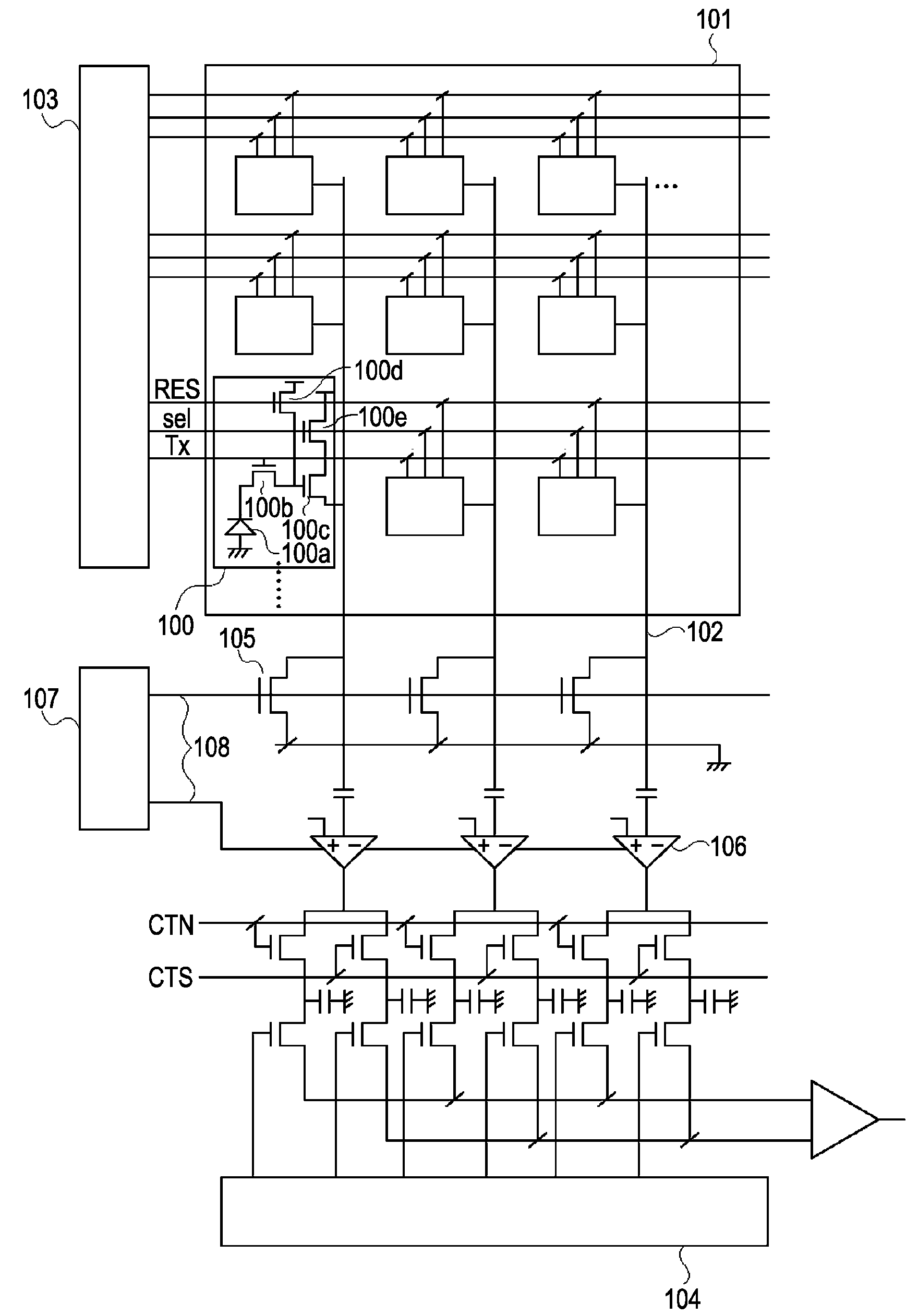
[0034]FIG. 1 is a conceptual diagram of a solid-state image pickup device according to a first embodiment.

[0035]The solid-state image pickup device includes pixels 100. The pixels 100 each include a photoelectric converter 100a, which is a photodiode in the first embodiment.

[0036]A transfer portion 100b transfers a charge of the photoelectric converter 100a to an input part of a pixel amplifier 100c. The pixel amplifier 100c amplifies and outputs a signal generated in accordance with the charge produced at the photoelectric converter 100a. A reset portion 100d resets the potential of the input part of the pixel amplifier 100c. A select portion 100e controls which signal is to be output to a corresponding one of vertical output lines 102. The foregoing elements can be configured as MOS transistors. The transistor serving as the pixel amplifier 100c is configured as a source follower circuit in combination with a load MOS transistor 105, which will be described separately below.

[0037]...

second embodiment

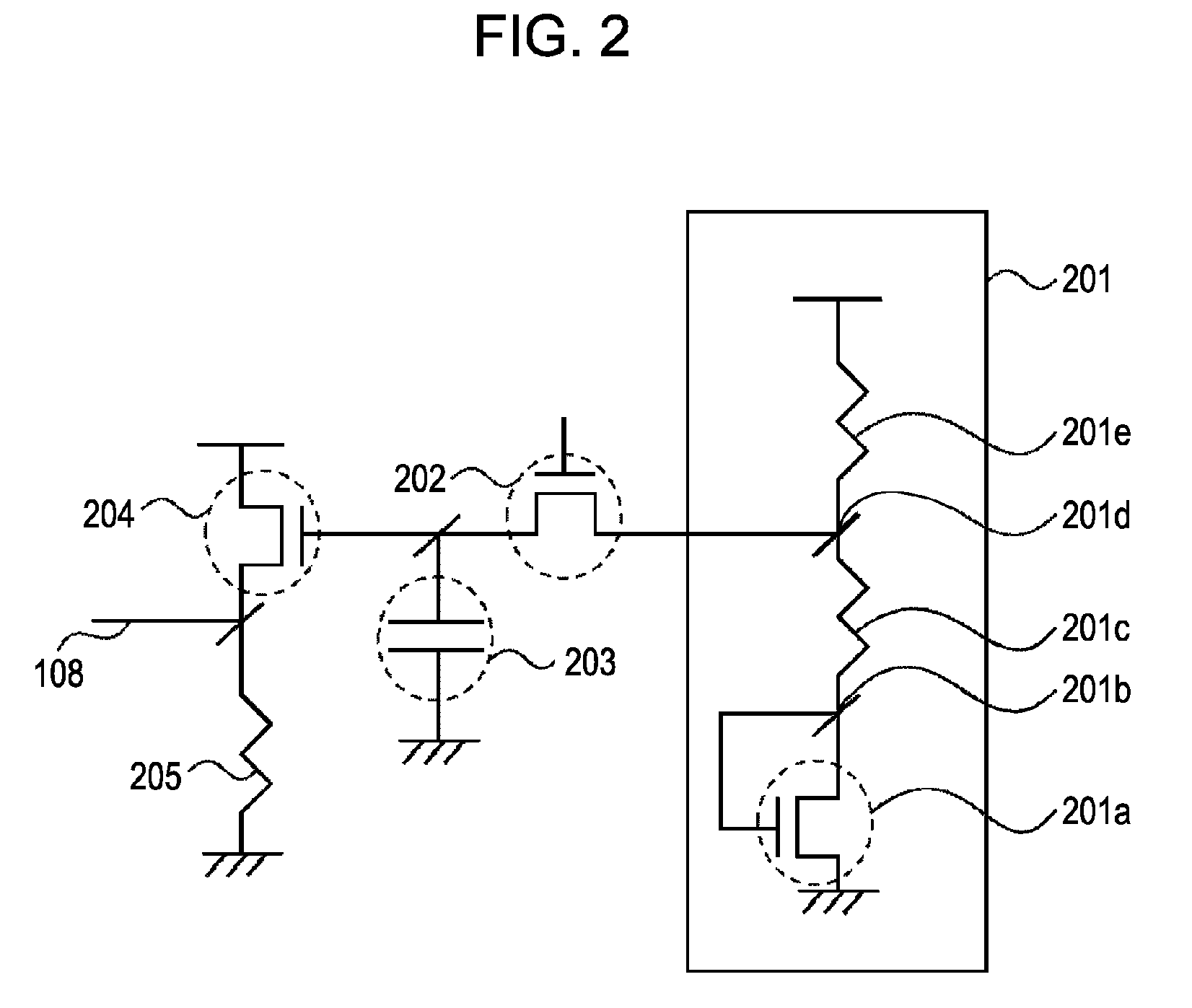
[0059]FIG. 4 is an equivalent circuit diagram of a voltage supply circuit according to a second embodiment. Elements similar to those of the first embodiment are denoted by the same reference numerals, and detailed descriptions thereof are omitted. In addition to the elements provided in the first embodiment, the voltage supply circuit of the second embodiment includes an operational amplifier circuit (a second amplifier circuit). Referring to FIG. 4, the voltage supply circuit includes an operational amplifier circuit 401 and a feedback path 402. A non-inverting input terminal of the operational amplifier circuit 401 and the voltage supply wire 108 (the output part of the voltage supply circuit) are connected to each other. The operational amplifier circuit 401 is provided between the voltage generator 201 and the sampling switch 202. The feedback path 402 connects an output node of the first amplifier circuit (the transistor 204 and the resistor 205) and an input node of the opera...

third embodiment

[0063]FIG. 5 is an equivalent circuit diagram of a voltage supply circuit according to a third embodiment. Elements similar to those in the first and second embodiments are denoted by the same reference numerals, and detailed descriptions thereof are omitted.

[0064]The third embodiment differs from the second embodiment in that the voltage supply circuit includes a first resistor 501 and a second resistor 502 connected in series on the output side of the transistor 204, with a connection node 503 between the resistors 501 and 502 being connected to the voltage supply wire 108. Operations of the switches and the like are the same as in the first and second embodiments. Also in the third embodiment, noises from the voltage generator 201 and the operational amplifier circuit 401 can be reduced by making the sampling switch 202 nonconductive during CDS processing. Further, in the third embodiment, the 1 / f noise generated in the transistor 204 appears at the output part of the voltage sup...


PUM


Abstract

A solid-state image pickup device includes a voltage supply circuit configured to supply a voltage to load MOS transistors provided to vertical output lines and columnar signal-processing circuits. The voltage supply circuit includes a first amplifier circuit configured to amplify a predetermined voltage supplied to an input part thereof from a voltage generator and to output an amplified voltage to a voltage supply wire, and a sample-and-hold circuit including a sampling switch provided on a path between the voltage generator and the input part and a hold capacitor configured to hold the voltage sampled by the sampling switch.

Description

BACKGROUND OF THE INVENTION [0001]1. Field of the Invention[0002]The present invention relates to solid-state image pickup devices, and more specifically to a technique of reducing noise occurring when reading is performed by a columnar signal-processing circuit provided for each pixel column of a solid-state image pickup device.[0003]2. Description of the Related Art[0004]Known amplifier solid-state image pickup devices include amplifier transistors provided in pixels thereof. Each amplifier transistor receives at a control electrode thereof a charge generated by a photoelectric converter, amplifies the charge, and outputs the amplified charge as a signal to a vertical output line, which is provided for each pixel column.[0005]In some cases, vertical output lines are provided with columnar signal-processing circuits that process signals. Japanese Patent Laid-Open No. 2003-051989 discloses an exemplary configuration in which each columnar signal-processing circuit includes an amplif...

Claims


Application Information

Patent Timeline
IPC IPC(8): H04N5/335H04N5/357H04N5/374H04N5/3745H04N5/378
CPCH04N5/217H04N5/378H04N5/3742H04N5/3577H04N23/81H04N25/617H04N25/767H04N25/75
Inventor SHINOHARA, MAHITO
Owner CANON KK
Why Eureka
Try Eureka